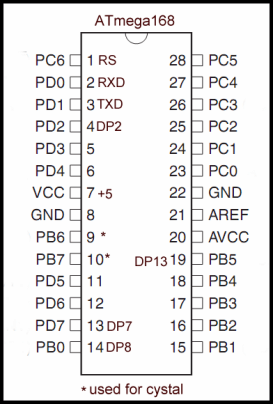
Fig.1 ATmega168 pin connections.
The following refers to Program Arduino Ports YouTube video related to this webpage.
Arduino Port Registers Revisited
The Arduino is a very popular microcontroller in the hobbyist market. Its programming is based on a modified C++. While this is good for some higher-level manipulations, it is very inefficient in many cases for direct hardware control.
Assembly language is very good for low-level control, but is tedious for the programmer on more complex functions. With both the Arduino and the PICAXE microcontrollers there are functions available that are virtually identical to assembly, but retain higher functions such as I2C interfacing and communicating with the terminal.
What I'm presenting in this series of projects is taking advantage of low-level direct control of I/O ports, but retaining full use of more complex functions. This enables one to save program code and increase execution speed. This is particularly important that on boot up the microcontroller takes immediate control of the electronics connected to its ports.
Far too often these programs are produced by programmers, but not hardware oriented people. I found this over the years to be a great headache dealing with specialized libraries for every component that may or may not work with every compiler change. I make it a habit to avoid libraries if possible and stick to the main functions.
Here I'm going to be using direct port manipulation to manipulate the microcontroller I/O. Programmers will stress not to do this due to portability and other issues. Again, we are interested in hardware control and often specialized hardware control. We are not dealing with a word processor.
If one is not familiar with bitwise functions see the following from the Arduino website:
Bit Math Tutorial by Cosine Kitty
PORTB register - 0b00100000
In Fig. 1 are the actual pin connections of an ATmega168 and corresponding port connection as explained at the bottom of the page. Above we see a binary representation of PORTB as seen to the program. "0b" on the left tells the compiler this is binary, the following zero or one is bit 7 (PB7) or most significant bit (MSB).
The zero or one on the right is PB0. 0-7 is eight bits or one byte. Digital pin 13 is PB5 counted from right to left and is set to a binary 1 - this outputs 5-volts to say a LED and turns it on. A binary zero is 0-volts and the LED goes off. In the case of PORTB PB6 and PB7 are attached to the crystal and unusable.
Each I/O port also a corresponding data direction register or DDR. The are also 8-bit and read from right to left.
PORTB DDR - 0b00100000
In this case a binary 1 on PB5 makes the corresponding I/O an output, while a binary 0 makes it an input. Writing data to an input programmed pin does nothing.
Working Example
Here is the first example, simply blinking an LED attached to digital pin 13:
/*
  Blink 1030 bytes - empty setup and loop 450
  580 bytes to blink an LED
 */

void setup() {
  // initialize digital pin 13 as an output.
  pinMode(13, OUTPUT); // 130 bytes
}

void loop() {
  digitalWrite(13, HIGH); // 218 bytes
  delay(1000); // 176 bytes
  digitalWrite(13, LOW); // 8 bytes
  delay(1000);  // 12 bytes
}
Something as simple as changing the state of an I/O pin takes 218 bytes while setting up that pin takes 130 bytes. Using this method to control say a stepper motor with 4 connections takes 16 lines of code and there's delays between each command. This is crazy and we are here to learn electronics.
/*
  Blink LED PIN13 with bitwise AND OR
  then write directly to port. 634 bytes.
  Won't compile error on arduino-1.6.7-windows on XP
 */

void setup() {
  DDRB = DDRB | 0b00100000;  // 4 bytes
}

void loop() {
   // set bit with bitwise OR
  PORTB = PORTB | 0b00100000; // 2 bytes
  delay(500); // 170 bytes
   // clear bit with bitwise AND
  PORTB = PORTB & 0b11011111; // 2 bytes
  delay(500); // 8 bytes
} // end loop
The above uses bitwise AND or a bitwise OR to clear and set bits. This has already saved lots of memory and functions the exact same way. Some claim use "DDRB = 0b00100000"; don't do this because it won't compile correctly if at all. Can we save more memory and do a better coding job? Yes we can!
/*
  Blink LED PIN13 with XOR write directly to port.
  628 bytes empty loop setup 444 bytes
  Won't compile error on arduino-1.6.7-windows on XP
 */

void setup() {
  DDRB = 0b00100000; // 4 bytes
  // pinMode(13, OUTPUT); // 130 bytes
  PORTB = PORTB & 0x00;  // 2 bytes
}

void loop() {
  // XOR PORTB with 0x20
  // toggles bit B.5 aka PIN13
  PORTB = PORTB ^ 0b00100000; // 8 bytes
  delay(500); // 170 bytes
} // end loop
Above we use a bitwise XOR to toggle bit BP5. We eliminated one delay() and a second line of AND code. We cleared (turned off all outputs) PORT DDR with a bitwise AND with zero. Can we save more memory? Yes we can!
/*
  Blink LED PIN13 with XOR write directly to port.
  502 bytes. Empty setup and loop 444 bytes
  Total program size 58 bytes from 628 bytes!
  Won't compile error on arduino-1.6.7-windows on XP
 */

 // Total program size 58 bytes from 628 bytes!
void setup() {
  DDRB = 0b00100000;  // 4 bytes
  PORTB = 0x00; // 2 bytes
}

void loop() {
  // XOR PORTB with 0x20 toggles bit B.5 aka DP13
  PORTB = PORTB ^ 0b00100000; // 8 bytes

  for (int i = 0; i <= 500; i++)   {
  // 1000 uSec = 1 mS
  delayMicroseconds(1000); // 26 bytes
  } // for loop 18 bytes
} // end loop
Above I've taken advantage of delayMicroseconds() that uses that uses 26 bytes (depends on compiler) with for loop using 18 bytes. Thus depending on compiler the entire program uses about 58 bytes.
This completes this short introduction.
Port registers allow for lower-level and faster manipulation of the i/o pins of the microcontroller on an Arduino board. The chips used on the Arduino board (the ATmega8 and ATmega168) have three ports:
B (digital pin 8 to 13)
C (analog input pins)
D (digital pins 0 to 7)
Note that here I won't address port C because the function is set by Arduino firmware. I'll only address PORTB and PORTD.
Each port is controlled by three registers, which are also defined variables in the arduino language. The DDR register, determines whether the pin is an INPUT or OUTPUT. The PORT register controls whether the pin is HIGH or LOW, and the PIN register reads the state of INPUT pins set to input with pinMode(). The maps of the ATmega8 and ATmega168 chips show the ports. The newer Atmega328p chip follows the pinout of the Atmega168 exactly.
DDR and PORT registers may be both written to, and read. PIN registers correspond to the state of inputs and may only be read.
PORTD maps to Arduino digital pins 0 to 7

DDRD - The Port D Data Direction Register - read/write
PORTD - The Port D Data Register - read/write
PIND - The Port D Input Pins Register - read only


PORTB maps to Arduino digital pins 8 to 13 The two high
bits (6 & 7) map to the crystal pins and are not usable

DDRB - The Port B Data Direction Register - read/write
PORTB - The Port B Data Register - read/write
PINB - The Port B Input Pins Register - read only
Ref. https://www.arduino.cc/en/Reference/PortManipulation
See How I got into Electronics
- PICAXE Projects
- YouTube videos:
- Simple Power Distribution for Prototype Board
- Program Arduino Ports for Speed and Control
- Digispark ATtiny85 with GPIO Expansion
- Safely Program H-Bridge Motor Controller
- Build H-Bridge Motor Control without Fireworks
- MOSFET H-Bridge for Arduino 2
- Arduino Projects Revisited Revised
- Programming ADS1115 4-Channel I2C ADC with Arduino
- Arduino uses ADS1115 with TMP37 to Measure Temperature
- Connect Arduino to I2C Liquid Crystal Display
- Arduino Reads Temperature Sensor Displays Temperature on LCD Display
- Arduino with MCP4725 12-bit Digital-to-Analog Converter Demo
- Videos
- Arduino with ADS1115 4-Channel 16-bit Analog-to-Digital Converter
- Arduino with MCP4725 12-Bit DAC
- Constant Current Circuits with the LM334
- LM317 Constant Current Source Circuits
- Introduction Hall Effect Switches, Sensors, and Circuits
- Microchip PIC related videos:
- How to Use K150 PIC Programmer
- Microchip PIC16F628A Basic H-Bridge Motor Control
- Microchip PIC16F628A Counts BCD on 8 LEDs
- PIC16F84A Operates H-Bridge Motor Control
- PIC16F84A Operates MOSFET H-Bridge
- Using Velleman K8048 PIC Development Board
- Microchip PIC16F84A H-Bridge Motor Control
- Microchip PIC16F628A Basic H-Bridge Motor Control
- PICAXE Operates H-Bridge Motor Controller
- PICAXE Micorcontroller Controls Motor Speed - Direction
- PICAXE Projects
- Arduino Port Registers Revisited
- Digispark ATtiny85 with MCP23016 GPIO Expander
- Safely Build Program a H-Bridge
- Build H-Bridge Motor Control Without Fireworks
- MOSFET H-Bridge for Arduino 2
- Web Master
- Gen. Electronics
- YouTube Channel
- Arduino Projects
- Raspberry Pi & Linux
- PIC18F2550 in C
- PIC16F628A Assembly
- PICAXE Projects
Web site Copyright Lewis Loflin, All rights reserved.
If using this material on another site, please provide a link back to my site.