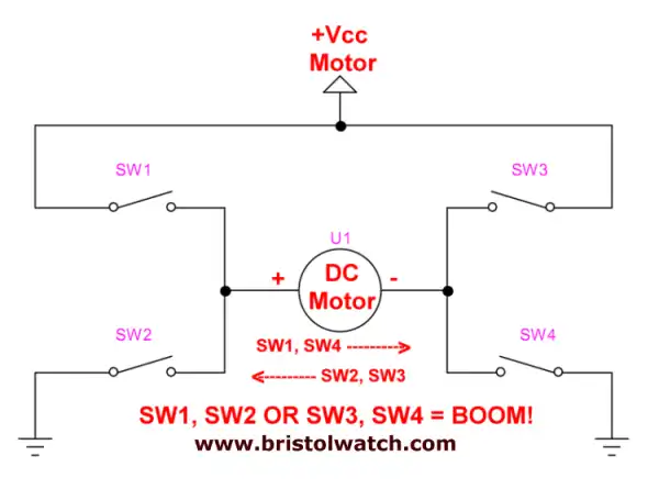
MOSFET H-Bridge Motor Control
by Lewis Loflin (lloflin2@gmail.com)
Permanent magnet Direct Current (DC) brushed motors have long served as electrical workhorses across an expansive array of voltage profiles and physical sizes. The mechanical direction of rotation in these components is determined exclusively by the polarity of the applied external voltage vector. If you reverse the physical polarity of the applied potential difference across the winding terminals, the motor's internal magnetic fields flip orientation, causing the rotor to reverse its direction of rotation.
One of the most elegant, robust, and widely deployed solid-state circuits engineered to achieve this electronic polarity reversal is the **H-bridge**. The name is derived directly from the graphic structure of its schematic blueprint, where a central bridge branch containing the load is suspended between two vertical switching legs.
The Mechanical Switch Analogy
To establish a solid baseline understanding before moving to solid-state semiconductors, Figure 1 diagrams a simplified H-bridge layout using two spring-loaded, single-pole, double-throw (SPDT) mechanical switches. The normally closed (NC) contacts are tied directly to the system ground common, while the normally open (NO) contacts are routed to the positive power rail (+12V DC). The two terminal lines of the DC motor are suspended directly between the common poles of these two switches.
In its normal resting state, the spring-loaded contacts keep both terminals of the motor tied directly to ground through the NC terminals. Because both sides of the inductive winding sit at an identical electrical potential (0V), no physical electron migration can occur, and the motor remains stationary.
When an operator depresses switch **SW1**, its internal contact breaks away from the grounded NC contact and snaps to the NO contact, injecting +12V into the left terminal of the motor. Because the right terminal remains grounded through the resting NC path of **SW2**, a closed loop is completed, forcing the motor to rotate at full speed in a counter-clockwise direction.
Releasing **SW1** and depressing **SW2** reverses this dynamic. Now, the right side of the motor winding is elevated to the +12V rail via the NO contact of **SW2**, while the left terminal is tied directly back to the ground line through the NC path of **SW1**. The resulting reversal of the electric field forces the motor to rotate in a clockwise direction. If an operator were to depress both switches simultaneously, both sides of the motor would elevate to the +12V rail, removing the potential difference and causing the motor to stop running.
Transitioning to Power MOSFETs
While mechanical switches work well for demonstrating basic operational logic, modern high-speed industrial automation and microcontroller interfaces require solid-state alternatives. H-bridge circuits can be built using discrete bipolar junction transistors (BJTs) or insulated-gate bipolar transistors (IGBTs). However, for low-to-medium voltage DC power control, **Metal-Oxide-Semiconductor Field-Effect Transistors (MOSFETs)** are generally preferred due to their exceptionally low internal conduction resistances.
Modern microcontrollers and single-board computers, such as the Raspberry Pi, operate on low-power 3.3V logic rails. This lower operating voltage requires the use of logic-level power MOSFETs that can achieve full channel enhancement at reduced gate-to-source potentials (VGS). Two highly effective, widely available components for these designs include:
- IRFZ44N (N-Channel): Rated safely up to 55V with an exceptionally low maximum static drain-to-source on-resistance (RDS(on)) of just 0.032 Ohms.
- IRF4905 (P-Channel): A complementary high-side P-channel device rated up to 55V with a maximum static drain-to-source on-resistance (RDS(on)) of only 0.02 Ohms.
When prototyping these high-current circuits on a test bench, it is highly recommended to place a current limiter on the main bench power supply and use a small, low-wattage test motor. Once the control logic and gate drive timings are verified, you can safely remove the current constraints and scale up to larger industrial DC loads.
Opto-Isolation vs. Common-Ground Topologies
Depending on the electrical noise environment and voltage differences between the logic and motor power rails, H-bridges are typically constructed using one of two primary grounding configurations:
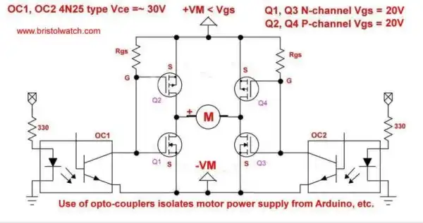
Figure 2 illustrates the deployment of high-speed opto-couplers (**OC1** and **OC2**). By using an internal infrared emitting diode optically coupled to an isolated phototransistor, the microcontroller's sensitive low-voltage ground plane remains completely isolated from the high-power inductive return lines of the motor loop. This configuration prevents inductive voltage spikes from feeding back into and destroying the logic controller.
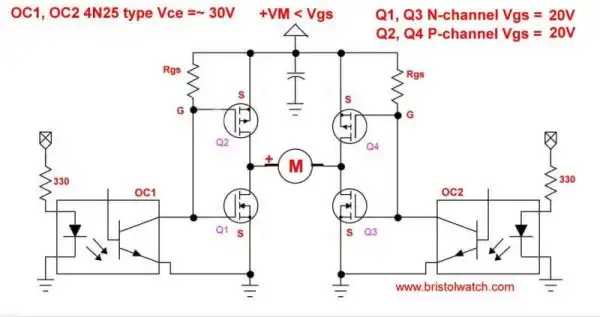
Figure 3 diagrams a simplified layout where a shared common ground plane is connected between the logic control stage and the high-power H-bridge drive network. While this configuration reduces component count, it requires careful PCB trace layout and decoupling to suppress electromagnetic interference (EMI).
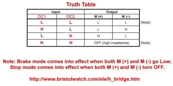
The control logic mapped in the truth table above (Figure 4) reflects standard operational modes derived from industrial H-bridge motor drivers, such as the Toshiba TA8050P assembly.
Analyzing H-Bridge Operational States via Electron Flow
To truly understand how the solid-state H-bridge controls current routing, we look to the physical **electron-flow model**, tracking the actual physical movement of electrons from the negative supply common, through the semiconductor matrices, and back to the positive rail.
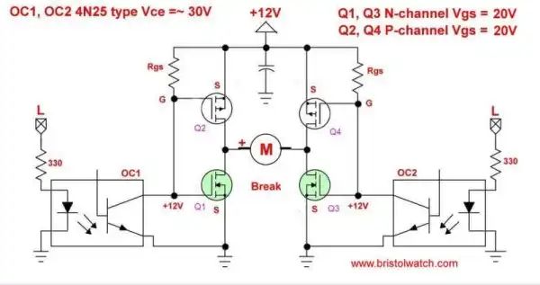
As illustrated in Figure 5, **Brake Mode** is established by turning off both high-side P-channel MOSFETs (Q1 and Q3) while biasing the gates of both low-side N-channel MOSFETs (Q2 and Q4) into a highly conductive, enhanced state. This grounds both sides of the motor windings through the low-resistance N-channel drain-to-source paths.
When the motor is spinning and power is cut, its kinetic momentum causes it to act as a generator. The resulting counter-electromotive force (counter-EMF) forces physical electrons to circulate in a short-circuit path through the enhanced channels and internal body diodes of Q2 and Q4. This creates an immediate electromagnetic counter-torque that rapidly brings the motor to a complete halt.
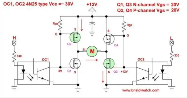
When a logic HIGH signal turns on opto-coupler **OC1** (Figure 6), high-side P-channel device **Q1** is switched off, while low-side N-channel device **Q3** is biased into conduction. This action establishes a continuous electron conduction path through the complementary pairs **Q2** and **Q3**.
Physical electrons exit the negative supply ground rail, travel up through the low-resistance enhanced channel of N-channel **Q3**, enter the motor winding from right-to-left, and return to the positive supply rail by passing through the conducting high-side P-channel **Q2**. This directional electron migration drives the motor in a clockwise direction.
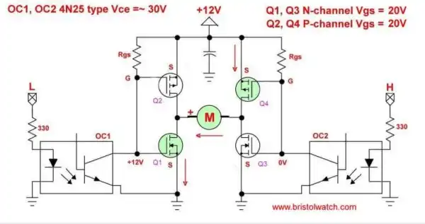
Conversely, when **OC1** is deactivated and **OC2** is driven active (Figure 7), **Q3** turns off and high-side **Q1** turns on, while **Q2** turns off and low-side **Q4** turns on. Physical electrons now emerge from the negative ground rail, travel up through N-channel **Q4**, enter the motor winding from left-to-right, and exit back to the positive power rail through P-channel **Q1**. Reversing the physical direction of electron injection through the winding reverses the mechanical torque vector, driving the motor counter-clockwise.
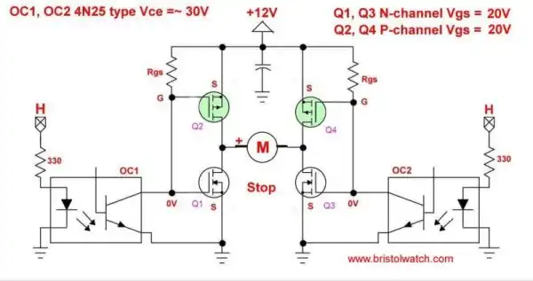
In **Stop Mode** (Figure 8), all four gate networks are biased off. The motor terminals are disconnected from both power rails, presenting a high-impedance state that allows the motor to passively coast to a stop under its own inertia.
The Shoot-Through Problem and System Optimization
A primary risk factor in H-bridge design is a destructive condition known as **shoot-through**, diagrammed in Figure 9 below.
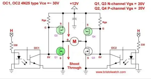
Power MOSFETs naturally exhibit a minute time delay when switching between conduction states due to internal parasitic gate capacitance. Shoot-through occurs if a high-side transistor (e.g., Q1) is turned on before the corresponding low-side transistor (e.g., Q2) has completely transitioned to its off state.
This overlapping conduction window creates a direct, ultra-low-resistance short circuit across the power supply rails. Electrons bypass the motor entirely and surge directly from ground to the positive rail through the vertical leg, causing massive current spikes, severe overheating, and catastrophic component failure. This risk increases significantly during high-frequency Pulse-Width Modulation (PWM) speed control or rapid directional changes.
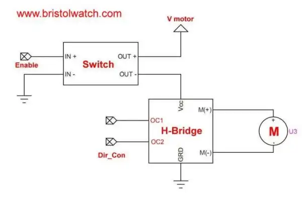
An effective hardware solution to eliminate this risk is adding a series-pass master power switch, as shown in Figure 10. By introducing a dedicated high-side control switch, you can cut the main power supply rail off entirely before changing H-bridge switching states, ensuring zero current flow during transition periods. This master switch can also be pulse-width modulated to provide smooth motor speed control.
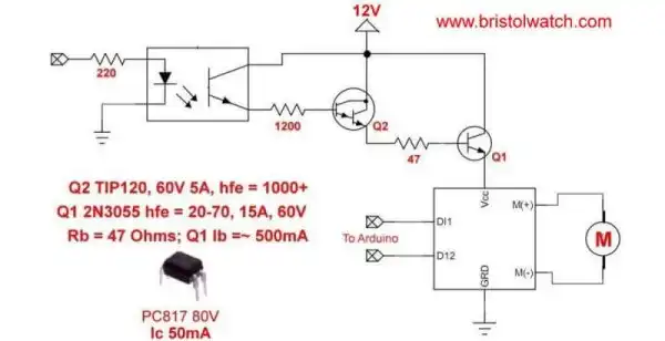
Figure 11 illustrates a robust, bench-tested design for a heavy-duty power switch utilizing a classic 2N3055 power transistor. For comprehensive layout instructions and formulas, see the full Design of a 10-Amp 2N3055 Based Power Switch tutorial.
Advanced Gate-Drive Considerations
When operating an H-bridge under real-world conditions, several practical electrical characteristics must be managed:
- Thermal Asymmetry: It is normal for high-side P-channel MOSFETs to run warmer than their low-side N-channel counterparts. This is a result of basic semiconductor physics: charge holes in P-type substrates possess lower mobility than free electrons in N-type substrates, giving P-channel devices a higher inherent RDS(on) for an equivalent die size.
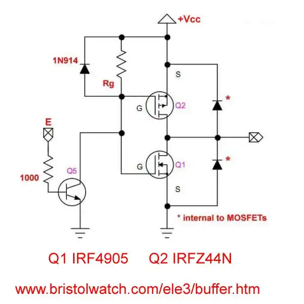
- Gate Resistance Tuning: The gate-to-source resistor (Rb) serves to discharge the internal gate-source parasitic capacitance (Ciss) to turn the MOSFET off. While a 10kΩ value is common for low-speed switching, dropping this resistance to 1kΩ (as shown in Figure 12) increases the discharge current path. This significantly speeds up turn-off times and sharpens the switching waveforms.
- Noise Suppression: Adding a high-speed 1N914 steering diode in parallel across the gate resistor helps suppress high-frequency transient noise spikes generated during rapid gate capacitance discharge cycles.
Highly Relevant Core Resources
To further advance your laboratory engineering capabilities in solid-state power switching and drive design, explore these 10 related modules:
- Design a 10-Amp 2N3055 Based Power Switch – High-current power isolation loops and saturation biasing math.
- LM317 High Power Constant Current Source Circuit – Build a heavy-duty, current-limited power supply rail to safeguard prototype drivers.
- LM317 Constant Current Source Circuits – Low-power precision current limiters for benchmark testing.
- Bipolar Junction Transistor (BJT) Switch Logic and Saturation – Foundation concepts covering base carrier injection and switching physics.
- How Diodes and Rectifiers Operate – Crystalline PN-junction mechanics, forward voltage drops, and flyback diode loop selection.
- High-Isolation Optocoupler Circuit Configurations – Using phototransistor chips to isolate low-power logic networks from inductive kickback.
- Silicon Controlled Rectifiers (SCR) Architecture and Trigger Gates – Unidirectional heavy power switching using multi-junction thyristor families.
- Understanding TRIAC Solid-State Power Switch Operations – Managing alternating current bidirectional loads via phase-fired triggers.
- Understanding Unijunction Transistors Theory and Operation – Analyzing negative resistance triggers and programmable relaxation loops.
- DIAC Waveform Generator and Trigger Circuits – Biasing two-terminal symmetrical trigger devices used in power gate control loops.