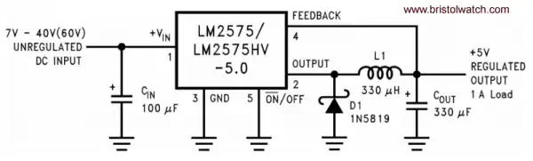
See LM2575 Simple Switching Voltage Regulators
Switching Regulars Configuration Review
by Lewis Loflin
Here I'll explain the basics behind switching voltage regulator configurations. This includes buck, buck boost, and buck boost inverting. By changing the capacitor, diode, and inductor configurations we change the type of regulator. All use transistor switching and assume an unregulated voltage input. I'll not be covering transformer based switching regulators.
To better understand inductor basics as it relates to switching regulators see Generating a Voltage with an Inductor.
The diode is known as a catch diode and must by a high speed Schottky or similar diode. A rectifier diode will not work.
Remember inductor basics that when a current flows through an inductor a magnetic field is induced (created) that can store energy in that field.
When the current is turned off the magnetic field will collapse inducing a new voltage in the coil, but of the opposite electrical polarity of the voltage that created it.
Also see Pulse Width Modulation Power Control for Microcontroller.
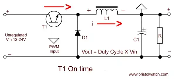
Fig. 1a
In Fig. 1a is a very basic buck step down configuration. When T1 is switched on current flows through L1 and partially charges C1 while creating a magnetic field in L1 storing part or most of the energy fed into the circuit. The amount of energy is proportional to the duty cycle of the pulse-width-modulation switching voltage on T1. The formula is Ton / (Ton + Toff) * Vin peak. Note the voltage polarity on L1.
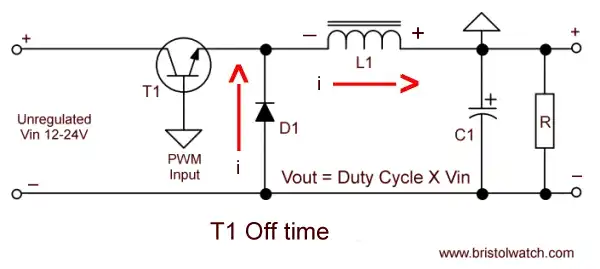
Fig. 1b
In Fig. 1b T1 is turned off and the magnetic field in L1 collapses inducing a voltage of opposite polarity to Fig. 1a. D1 then conducts transferring that energy charging the C1 output capacitor.
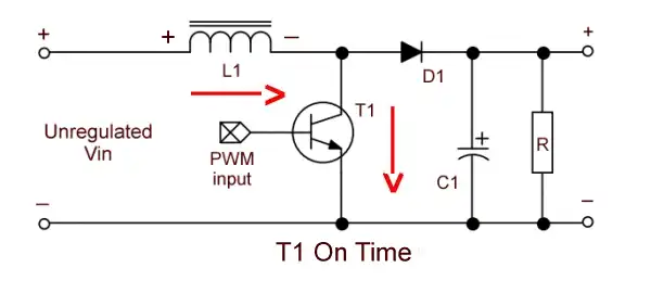
Fig. 2a
In Fig. 2a we have a buck boost configuration producing a higher output voltage than the input voltage. When T1 is switch on current flows through L1 and through T1 to ground generating once again energy storage in L1's magnetic field. Note the voltage polarity on L1.
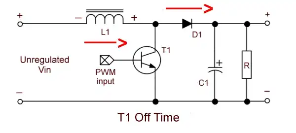
Fig. 2b
In Fig. 2b T1 is switched off the magnetic field in L1 collapses inducing a voltage of opposite polarity. This voltage is in series polarity with the input voltage and they add, charging C1 though D1 at a higher voltage than the input voltage. Again note the voltage polarity on L1.
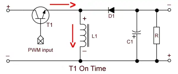
Fig. 3a
In Fig. 3a we have the buck-boost inverting configuration. When T1 is turned on current flows through T1 and L1 as shown. Tote the voltage polarity on L1. Voltage to C1 is blocked by D1 thus no charging voltage.
Fig. 3b
In Fig. 3b T1 is turned off and the magnetic field in L1 collapses inducing a new voltage of the opposite polarity. D1 now conducts charging up C1 producing a negative output voltage of opposite polarity from the input.
As a final note the pulse-width-modulation frequency can be very high reducing inductor and capacitor size. A LM2575T for example uses a frequency of 52kHz.
That concludes this brief introduction to switching voltage regulator configurations.
- Operation switching power supplies and transformer connection tutorials:
- Generating High Voltage with an Inductor
- Arduino Buck Switching Voltage Regulator Demo Only
- Switching Regular Configuration Review
- LM2575 Simple Switching Voltage Regulators
- Voltage Buck-Boost Transformer Connections Tutorial
Other Circuits
- Hall Effect Magnetic Switches and Sensors
- Transistor-Zener Diode Regulator Circuits
- Build an Adjustable 0-34 volt power supply with the LM317
- Coils for Highly Selective Crystal Radio
- Neon (NE-2) Circuits You Can Build
- Understanding Xenon Flashtubes and Circuits
Web site Copyright Lewis Loflin, All rights reserved.
If using this material on another site, please provide a link back to my site.