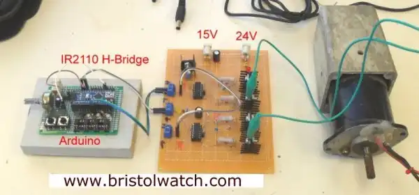
Fig. 1 My IR2110 H-Bridge control board connect to Arduino and motor.
Click above for larger image.
Arduino Controlled IR2110 Based H-Bridge High Voltage Motor Control
by Lewis Loflin
Fig. 1 is my final build of an Arduino controlled IR2110 based h-bridge motor control.
Youtube video: Arduino Controlled IR2110 Based H-Bridge High Voltage Motor Control
Note any corrections, comments, or questions email me at lewis@bvu.net.
The IR2110 is a popular h-bridge half driver. It is designed to drive high voltage MOSFET and IGBT circuits. It does this without the use of p-channel MOSFETs or photovoltaic opto-couplers.
The circuit generates HIGH side MOSFET gate voltage from a diode, bootstrap capacitor combination.
Related IGBT Based High Voltage H-Bridge DC Motor Control.
In this case the IR2110 is an 14-pin DIP IC and I used 2 for a complete h-bridge. The schematic to each half is identical.
I used the 15V MOSFET/IGBT gate voltage with a 5-volt regular to supply the digital voltage (VDD) of 5V. The motor power supply is separate and is limited by the MOSFETs used and motor voltage up to 500-volts.
The web is filled with the same schematic with various problems and not a clue on how it operates. Frustrating still little information on how to operate the high voltage side MOSFET.
Mine was built, tested and working. I'll cover the process and will explain theory of operation. I'll also present the Arduino code.
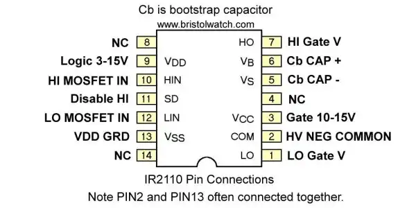
Fig. 2 IR2110 half h-bridge driver pin connections.
Input Pin Connections
Fig. 2 illustrates the electrical pins on a IR2110. Their uses are as follows:
First I'll discuss pins 9-13 what I consider the digital control inputs. Pins 1-7 I consider the driver outputs and will be explained below.
Pin 9 or VDD is the digital logic positive voltage range 3-15V. This enables the use of CMOS or LS TTL logic.
The VDD voltage depends on the type of logic connected to the inputs. I used a 5V Arduino so I connected 5V from a voltage regulator.
If using 3V logic such as Raspberry Pi GPIO connect to 3V. If using CMOS logic at say 12V connect VDD to 12V.
Pin 10 or HIN controls the output on pin 7 labeled HO that controls the HIGH side MOSFET. This input must be pulse-width-modulated as explained below.
Pin 12 or LIN controls the LOW side MOSFET connected to pin 1 LO. A HIGH outputs 10-15V on pin 1 turning on the LOW side MOSFET.
Pin 11 or SD will disable all outputs when HIGH. This is mostly connected to digital ground.
Pins 10, 11, and 12 all have Schmitt trigger inputs and internal pull down resistors.
Pin 13 or VSS is the digital power supply negative ground. This is often connected to motor supply HV voltage ground COM or pin 2.
Pins 8 and 14 no connection.
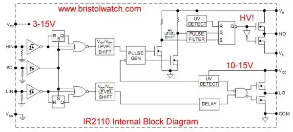
Fig. 3 Internal block diagram IR2110 half h-bridge circuit.
Fig. 3 is the internal block diagram of the IR2110. The digital control is on the left. Note the digital common VSS is separate from the motor supply common COM.
Note the VDD to VCC level shifting circuitry. VCC is MOSFET gate drive voltage at pin 3. The entire upper right of the block diagram is "floating" and isolated from the lower voltage circuits.
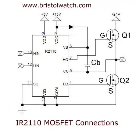
Fig. 4 Simplified IR2110 output MOSFET connections.
Output Pin Connections
Now comes the tricky part the output. The IR2110 uses to "bootstrap" capacitor to supply the gate turn on voltage for MOSFET Q1. MOSFETs Q1 and Q2 are connected in a "totem pole" configuration.
Pin 7 supplies the gate drive voltage for HIGH side MOSFET Q1. Pin 1 supplies the gate drive voltage for LOW MOSFET Q2.
Notice the internal "totem pole" outputs from LO and HO within the IR2110. VCC pin 3 is 10-15V gate drive voltage. Each have internal under voltage (UV) detectors. When the gate voltage drops below ~8.5V outputs are turned off.
Capacitor Cb is charged through a diode from VCC to 15V. Internal transistor "A" will switch the capacitor voltage to gate Q1. Cb can no longer charge from VCC until Q1 is turned off.
It is the charge-discharge of Cb connected across Q1 that keeps Q1 turned on.

Fig. 5 HIGH side MOSFET circuits using IR2110.
Fig. 5 is a close up look at the HIGH MOSFET power circuit. RL represents the load (motor for example) and the LOW side MOSFET turned on at the other half of the h-bridge.
Capacitor Cb in my circuit is a 0.22uF or 220n. It is charged to 15V through diode D1. In my case I used a 1N4007. For high speed switching a UF4007 high speed diode. must be used.
D1 also serves to block the motor drive voltage from 15V VCC.
The capacitor charges to 15V across VB and VS when Q1 is off. VS is connected to Q1 source connection.
When a HIGH is input to HIN the voltage at VB is switched to pin HO turning on Q1. Once Q1 is turned on the motor voltage appears at Q1 source preventing any further charging of Cb.
Cb will discharge the rate related to MOSFET leakage, etc. Most internet sites connect a 1K resistor across Q1 gate-source, I removed it. They also connected a 22uF electrolytic across Cb I removed that.
They also failed to bypass VCC so I added 22uF capacitor to ground. I removed a 22uF bypass capacitor across VDD as not needed.
Diode D2 was a 1N4007 in the test circuit. I used a 1N4148 high speed diode in the final circuit.
MOSFETs tested: IRFZ40 - VDS = 60V; ID = 36A and IRFZ44N - VDS = 55V; ID = 49A
The following from IR application note AN978-b.
VDD is 3-15V, the output stage is implemented either with two N-Channel MOSFETs in totem pole configuration.
Each IR2110 MOSFET can sink or source gate currents up to 2A, depending on the MGD. MGD stands for MOS-gate-driver.
To quote in regards to VB, VS, and HO:
This channel has been built into an "isolation tub" capable of floating from 500 or 600V to -5V with respect to power ground (COM). The tub "floats" at the potential of VS, which is established by the voltage applied to VB. Typically this pin is connected to the source of the high side device...
The gate charge for the high side MOSFET is provided by the bootstrap capacitor which is charged by the 15V supply through the bootstrap diode during the time when the device is off.
The use of pulses greatly reduces the power dissipation associated with the level translation. The pulse discriminator filters the set/reset pulses from fast dv/dt transients appearing on the VS node so that switching rates as high as 50V/ns in the power devices will not adversely affect the operation of the MGD.
This channel has its own undervoltage lockout ( on some MGDs) which blocks the gate drive if the voltage between VB and VS, i.e., the voltage across the upper totem pole is below its limits (typically 8.7/8.3V). The operation of the UV lockout differs from the one on VCC in one detail: the first pulse after the UV lockout has released the channel changes the state of the output. The high voltage level translator circuit is designed to function properly even when the VS node swings below the COM pin by a voltage indicated in the data sheet, typically 5 V.
The following in my view is nonsense. I used a single 15V supply for VCC and the motor supply voltage. 12V should also work. It worked just fine with my h-bridge.
1. Gate voltage must be 10-15V higher than the drain voltage. Being a high side switch, such gate voltage would have to be higher than the rail voltage, which is frequently the highest voltage available in the system.
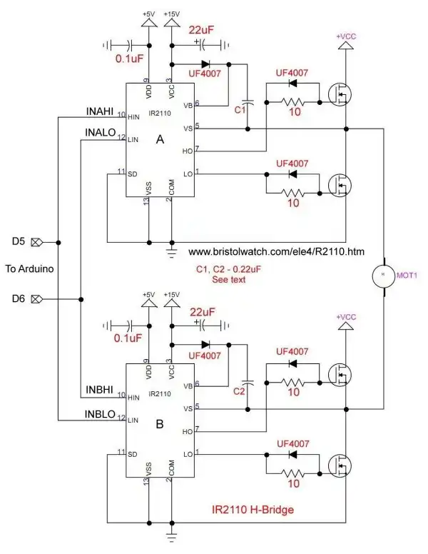
Fig. 6 Final h-bridge schematic using 2 IR2110a.
Click above for larger image.
Final schematic above, Arduino code below.
In the code below I used 4 Arduino pin D5-D8. They inputs above can be cross-wired as shown using just D5 and D6.
Arduino Code
/*
 Driver demo routine for IR2110 h-bridge.
 2 NO pushbutton switches connected D2, D3 to GND.
 by Lewis Loflin lewis@bvu.net
 https://www.bristolwatch.com/ele4/IR2110.htm
*/

#define INAHI 5 // pwm input A HI MOSFET
#define INBHI 6 // pwm input B HI MOSFET
#define INALO 7 // input A LO MOSFET
#define INBLO 8 // input B LO MOSFET

#define POT 0

#define SW1 2
#define SW2 3

int val;

void setup() {
  pinMode(INAHI, OUTPUT);
  pinMode(INBHI, OUTPUT);
  pinMode(INALO, OUTPUT);
  pinMode(INBLO, OUTPUT);

  digitalWrite(INAHI, LOW);
  digitalWrite(INBHI, LOW);
  digitalWrite(INALO, LOW);
  digitalWrite(INBLO, LOW);

  pinMode(SW1, INPUT);
  pinMode(SW2, INPUT);

  pinMode(SW1, INPUT_PULLUP);
  pinMode(SW2, INPUT_PULLUP);
}

void loop() {

  analogWrite(INAHI, 0);
  analogWrite(INBHI, 0);

  // INAHI HIGH and INBLO HIGH
  // INALO LOW and INBHI LOW
  while (!digitalRead(SW1))   {
    digitalWrite(INALO, LOW);
    digitalWrite(INBHI, LOW);
    val = analogRead(POT)/ 4 ;
    analogWrite(INAHI, val);
    digitalWrite(INBLO, HIGH);
  }

  // INAHI LOW and INBLO LOW
  // INALO HIGH and INBHI HIGH
  while (!digitalRead(SW2))   {
    digitalWrite(INAHI, LOW);
    digitalWrite(INBLO, LOW);
    val = analogRead(POT)/ 4;
    analogWrite(INBHI, val);
    digitalWrite(INALO, HIGH);
  }

} // end loop
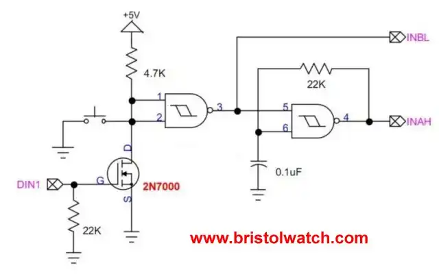
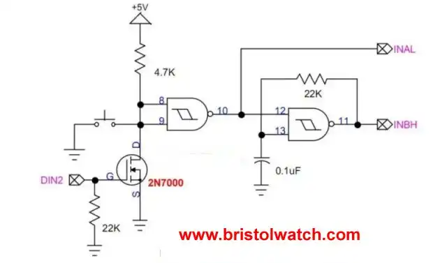
Upgrade new input circuits don't use the above Arduino code
Video link: IR2110 High Voltage H-Bridge Input Circuit Upgrade
Use only two control pins.
Caution: never turn on both h-bridge input at the same time! Program a dead space between direction changes.
Summary of Default PWM Frequencies for Arduino Nano:
Pins 3, 5, 6, 11: ~976 Hz (Timer0 and Timer2, Fast PWM, prescaler = 64);
Pins 9, 10: ~490 Hz (Timer1, Fast PWM, prescaler = 64).
The squarewave frequency output from the CD4093 pin4 and pin11 are based on the value of feedback resistor R and timing capacitor C.
With a value of C = 0.1uF and R = 22K then the output is 1200Hz. This was a live test not a theory. The formulas given in the spec sheet are useless for this setup.
In the following test values R was fixed at 10K and the frequency out was measured on a frequency counter. This was measured connected to the H-bridge circuit as it was operating.
C = 0.1uF, F = 2.58kHz;
C = 0.047uF, F = 5kHz;
C = 0.015uF, F = 15.25kHz;
C = 0.0056uF, F = 30.5kHz;
C = 0.0047uF, F = 40kHz.
- Quick navigation of this website:
- You Tube Channel
- Basic Electronics Learning and Projects
- Homepage Lewis Loflin
- Follow on X
- Skeptic Site
- Religion 1
- Religion 2
- Coils for Highly Selective Crystal Radio
- Neon (NE-2) Circuits You Can Build
- Understanding Xenon Flashtubes and Circuits
- Hall Effect Magnetic Switches and Sensors
- Transistor-Zener Diode Regulator Circuits
- Build an Adjustable 0-34 volt power supply with the LM317
- Simple 2 Transistor LED Flasher Circuit
- LM2575 Simple Switching Voltage Regulators
- LM317 Constant Current Source for Lighting LEDs
- IGBT Based High Voltage H-Bridge DC Motor Control
- Arduino Controlled IR2110 Based H-Bridge HV Motor Control
- Understanding Unijunction Transistors Theory Operation
- Arduino Measures Current from Constant Current Source
- Constant Current Source Theory Testing
- Review Ohm's Law for Trouble-Shooting CCS Circuits
- Arduino Power Magnetic Driver Board for Stepper Motors
- Arduino Controlled Power Constant Current Source
- Theory and Operation of Capacitors
Related video to above:
- Measure Current from Constant Current Source with Arduino
- Constant Current Source Multimeter Trouble Shooting
- Ohm's Law Review for Constant Current Source
- Arduino Unipolar Stepper Motor Driver Board with Arduino Code
- Arduino Controlled Constant Current Source
- LM317 Adjustable Current Boost Power Supply
- Constant Current Circuits LM334, LM317
- Build LM317 0-34 Volt Power Supply
- LM334 Constant Current Source with Resistive Sensors
- LM317 High Power Constant Current Source Circuit
- LM317 Constant Current Source Circuits
- Test SCRs and Triacs
- Basic MOSFET Transistor Test Circuits
- High Voltage MOSFET Switching Circuits
- 3 Amp LM741 Op-Amp Constant Current Source
- Current Limiter Testing of Zener Diodes
- Current Limiter for Opto-Coupler Inputs
- LM317 CCS for Light Emitting Diodes
Web site Copyright Lewis Loflin, All rights reserved.
If using this material on another site, please provide a link back to my site.