Fig. 1 USB oscilloscope output from a CD4040 frequency divider.
Click for larger image.
CD4040 12-stage Binary Counter with DS1307 RTC Time Base
by Lewis Loflin
Full size image of above. See cd40.jpg.
This webpage will focus on the CD4040BC 12-Stage Ripple Carry Binary Counter. I will explain how the device operates and will use as a time base.
As a clock source I used the output from a DS1307 RTC square wave output. For that part see DS1307 RTC with a CD4040 as a Precision Time Base.
This works the same with a 32kHz oscillator circuit. The CD4060 is setup to use its own oscillator crystal.
This does not require a DS1307. One can use a stand alone oscillator circuit. The CD4040s can be connected in series - Q12 output to the input of another CD4040.
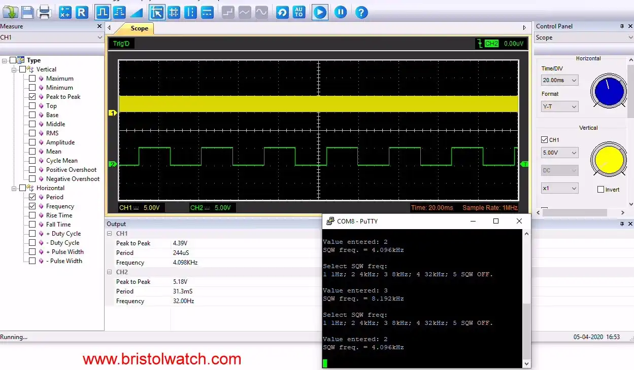
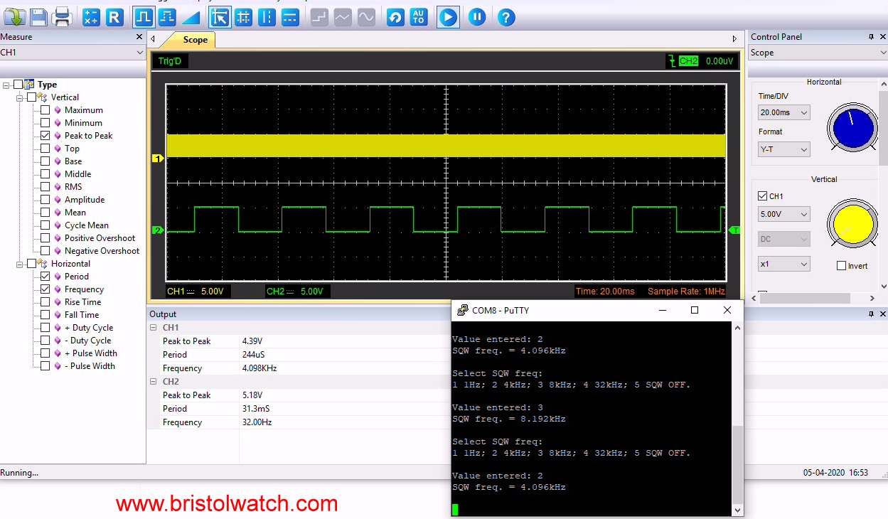
Fig. 8 is the output to my USB oscilloscope and the frequency select program for the DS1307 on PuTTY.
Channel 1 is the 4,096Hz output from the DS1307 as selected by the menu on PuTTY. Channel 2 is connected the Q7 (pin 4) of a CD4040 used as a frequency divider.
The oscilloscope is triggered on channel from the 32Hz output from pin 4 (Q7) from a CD4040.
But what is the Q7 output? The spec sheet is vague and hard to understand for beginners. Let us look closer.
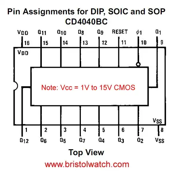
Fig. 2 CD4040 package outline pin connections.
Fig. 2 illustrates the 16-pin DIP package. Besides GND and +Vcc we have 12 outputs labeled Q1-Q12. These can be thought of as powers of 2.
Pin 9 is the clock input. Pin 10 is reset. When HIGH flip-flops Q1-Q12 are cleared all outputs go to LOW. I tied this LOW to GND.
From the spec sheet:
CD4020BC 14-Stage Ripple Carry Binary Counters
CD4040BC 12-Stage Ripple Carry Binary Counters
CD4060BC 14-Stage Ripple Carry Binary Counters
Voltage range: 1V to 15V. Speed 8mHz. Schmitt trigger clock input.
Low power TTL compatibility:Fan out of 2 driving 74L or 1 driving 74LS loads.
The CD4020BC, CD4060BC are 14-stage ripple carry binary counters, and the CD4040BC is a 12-stage ripple carry binary counter. The counters are advanced one count on the negative transition of each clock pulse. The counters are reset to the zero state by a logical "1" at the reset input independent of clock.
The CD4020 and CD4060 while having 14 stages still have only 12 outputs limited by their 16-pin DIPs.
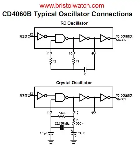
Fig. 3 CD4060BC oscillator connections.
Fig. 3 illustrates the oscillator section built into a CD4060BC.
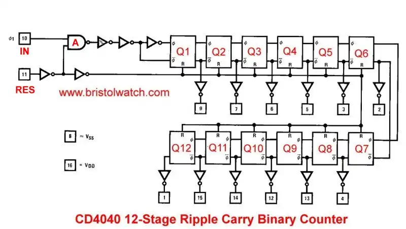
Fig. 4 Internal block diagram to CD4040BC.
Fig 4 is the internal block diagram of a DC4040BC. Pin 10 is the clock input, pin 11 is reset. When RES is HIGH this is inverted, NAND gate A is disabled. The this is inverted again placing a HIGH on each Q flip-flop reset. All outputs go LOW. All outputs are also buffered. The clock circuit includes Schmitt trigger input.
This is a frequency divider. The frequency output depends on which Q output is used.
To calculate the division raise 2 to the power of Q. For example for Q12 is 2^12 = 4,096. With a frequency input (pin 10) of 4096Hz Q12 output at pin 1 is 1Hz.
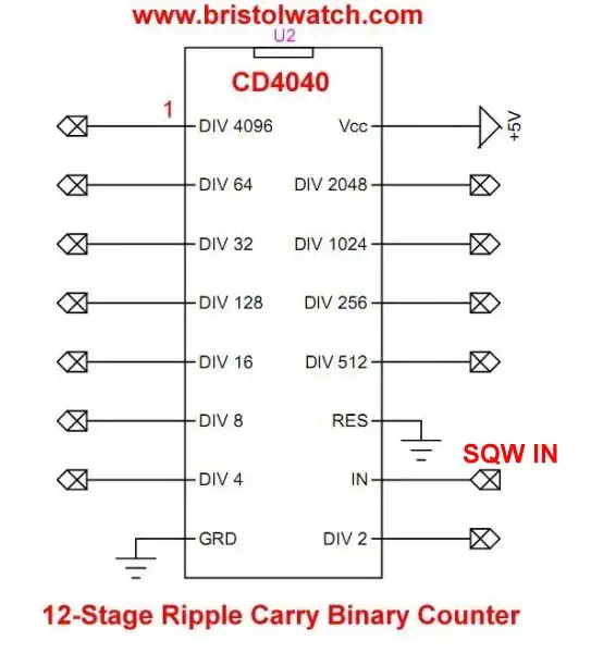
Fig. 5
In Fig. 5 I have labeled the outputs to divisions by 2 as opposed to Q1-Q12.

- MOSFET-Transistor Drivers with TC4420 and TC4429, IGBTs, etc.
- Introduction TC4420-TC4429 MOSFET Drivers
- Use TC4420 MOSFET Driver for Simple H-Bridge Circuit
- TC4420 MOSFET Driver Various Circuits
- TC4420 MOSFET Driver Replacement Circuits
- Test Power MOSFET Transistors, IGBTs
- Insulated Gate Bipolar Transistor IGBT Circuits
- Issues on Connecting MOSFETs in Parallel
- TC4420 MOSFET Driver Replacement Circuits
- TB6600 Stepper Motor Driver with Arduino
- Interfacing Microcontrollers to CMOS and MOSFET Circuits
- Simplified CMOS-MOSFET H-Bridge Circuit
- Tri-State H-Bridge using CD4093B CMOS Circuit
- Common Collector Opto-Isolated Bipolar Transistor Switches
- Compare 2N3055 MJE10005 Transistor Power Switches
- Connecting PCF8574P GPIO Expander to Raspberry Pi
- Programming PCF8574P 8-bit I-O Expander with Arduino
- DS1307 RTC with a CD4040 as a Precision Time Base
- CD4040 12-stage Binary Counter with DS1307 RTC Time Base
- Pt. 1 Interfacing Microcontrollers to CMOS and MOSFET Circuits
- Pt. 2 Simplified CMOS-MOSFET H-Bridge Circuit
- Pt. 3 Tri-State H-Bridge using CD4093B CMOS Circuit
- Pt. 1 TB6600 Stepper Motor Driver with Arduino
- Pt. 2 Program TB6600 Stepper Motor Driver with Arduino
- TB6600 Stepper Motor Driver with Arduino
- Off Site:
- Web Master
- Tri-Cities VA-TN
- General Science
- Hobby Electronics
- US Constitution
- Christianity 101
- Religious Themes
© Copyright 2018 Lewis Loflin E-Mail