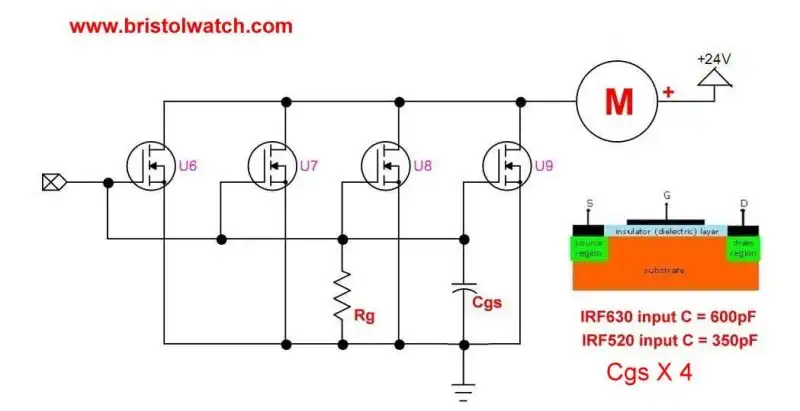
Fig. 1 N-channel MOSFETs connected in parallel.
Connecting MOSFETs in Parallel
by Lewis Loflin
The following slides are covered in the YouTube video above.
Several visitors to this website have tried to connect power MOSFET transistors in parallel in order to switch a higher power load. Here I'll explore that issue and why problems may arise.
View YouTube video Issues on Connecting MOSFETs in Parallel.
Fig.1 illustrates 4 n-channel MOSFETs connected in parallel. At issue is Rg the gate bleeder resistor. Due to MOSFET construction with a very thin dielectric insulator between gate-source can create considerable capacitance. Rg is designed to bleed of the charge on the gate when turned on at assure turn off.
The problem is when MOSFETs are connected in parallel the capacitance is multiplied and that is where the trouble begins. Going by the specification sheet one can Cgs. Note the left side of Fig. 1 on how the MOSFET is constructed.

Fig. 2 Construction of N-channel MOSFET.
Fig. 2 illustrates the construction of a typical n-channel MOSFET. A positive charge on the gate electrode draws negative charges to the gate creating a conductive pathway. This would seem to create even more capacitance as the insulator separates the gate from the conductive channel. A capacitor after all is two conductors separated by an insulator.
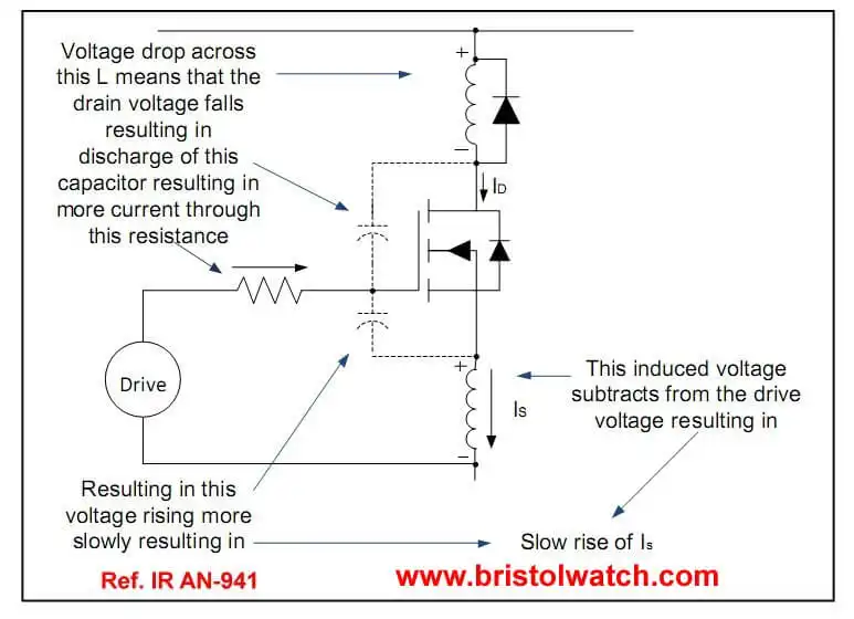
Fig. 3 Effects of stray capacitance in power MOSFET switching.
Fig. 3 taken from International Rectifier shows the problems of stray capacitance and inductance with a MOSFET. This can easily distort the drive signal creating noise and switching problems.
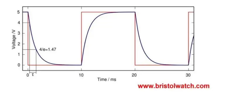
Fig. 4 Input capacitance distorts square wave drive signal to MOSFET.
The result is a nice clean digital pulse from say an Arduino microcontroller has a lagging turn on and lagging turn off. This charge curve is common in capacitive-resistive circuits.
Trying to switch on-off multiple MOSFET at one time becomes a challenge. Let's look more closely at how to address possible solutions.
Update Dec. 2019. Many micro-controllers today are using 3.3-volt Vcc. This is also true of Raspberry Pi. I found two MOSFETs that work at 3.3-volts.
The IRFZ44N is an N-channel device rated at 55V and RDS(on) resistance of 0.032 Ohms max. The other is a P-channel device rated at 55V and a RDS(on) of 0.02 Ohms max.
See the following spec sheets:
Also see Test Power MOSFET Transistors, Results, Observations
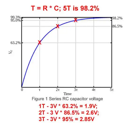
Fig. 5 Charge curve for 3-volt MOSFET square wave drive pulse.
Many hobbyists use a 3-volt microcontroller or in the case of Raspberry Pi 3-volt IO is the norm. Gate-source capacitance becomes a real problem at lower voltages in the reliable switching on-off of multiple paralleled MOSFETs.
Let's note a charge curve that T (for time) is C * R. The charge curve is not linear. The fastest voltage rise is the first period T, then the rates greatly slows down. 5 times T is considered fully charged.
The exact opposite for turn-off or discharge.
Some MOSFETs will turn on at 3-volts, but many that I've tested fully turn on from 3.5 to 4.3 volts. This is further compounded that in the real world every MOSFET is not 100% identical even if the same part number.
As Fig. 5 at 3-volts it will take 3T to come up near 3 volts to turn on a MOSFET. More MOSFETs more capacitance, longer time period for T.
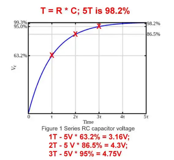
Fig. 6 Charge curve for 5-volt MOSFET square wave drive pulse.
In Fig.6 with 5-volts 1T produces 3.6V turning on most MOSFETs. Somewhere between 1T and 2T assures most MOSFETs such as the IRF630 will turn fully on.
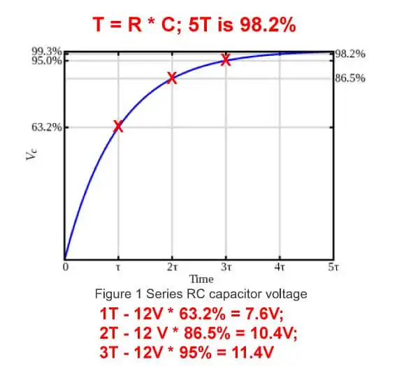
Fig. 7 Charge curve for 12-volt MOSFET square wave drive pulse.
Fig. 7 illustrates the use of a 12-volt pulse. 1/2 T will switch on all MOSFETs. This may not be so good for turn off as the higher voltage discharge may delay turn off.
![]()
Fig. 8 MOSFET based driver circuit.
While we can't reduce Cgs other than using MOSFETs with a lower Cgs, the best solution is to reduce R. The circuit in Fig. 8 can be a solution.
A HIGH input will switch on Q2 providing a fast low-resistance pulse providing the rush of current need to switch on the 4 MOSFETs. A low input turn on Q1 providing a very low resistance discharge path.
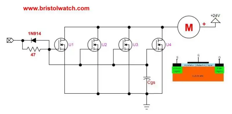
Fig. 9 Parallel MOSFETs configuration 1.
Fig. 9 illustrates parallel MOSFETs with gates connected together and a single charge/discharge resistor. The diode suppresses noise generated as current rushes through the resistor.
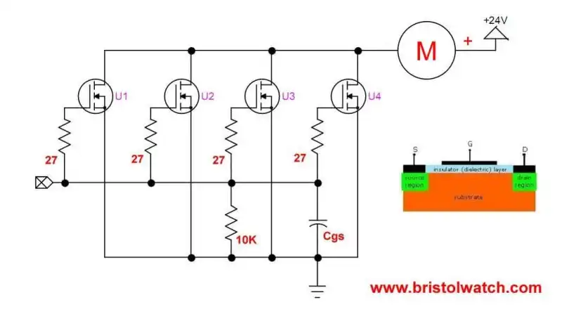
Fig. 10 Parallel MOSFETs with individual gate resistors.
Fig. 10 illustrates a resistor on each individual MOSFET gate. With either Fig. 9 or 10 include the 10K resistor is included so the MOSFETs are assured to be turned off at power up.
Have fun.
- Quick navigation of this website:
- Basic Electronics Learning and Projects
- Basic Solid State Component Projects
- Arduino Microcontroller Projects
- Raspberry Pi Electronics, Programming
- Comparator Theory Circuits Tutorial
- Zero-Crossing Detectors Circuits and Applications
- Improved AC Zero Crossing Detectors for Arduino
- Photodiode Circuits Operation and Uses
- Photodiode Op-Amp Circuits Tutorial
- Issues on Connecting MOSFETs in Parallel
- MOSFET DC Relays Using Photovoltaic drivers
- Optocoupler Input Circuits for PLC
- All NPN Transistor H-Bridge Motor Control
- Photo Voltaic Tutorial MOSFET Output Solid State Relays
- Optical Isolation of H-Bridge Motor Controls
- Design 10-Amp 2N3055 Based Power Switch
- TA8050P H-Bridge Motor Control
- Connecting Crydom MOSFET Solid State Relays
- H11L1, 6N137A, FED8183, TLP2662 Digital Output Optocouplers
- Arduino
- Arduino PWM to Analog Conversion
- Arduino Analog Digital Conversion Voltmeter
- Better Arduino Rotary Encoder Sensor
- Simple 3-Wire MAX6675 Thermocouple ADC Arduino Interface
- Hall Effect Magnetic Switches and Sensors
- Transistor-Zener Diode Regulator Circuits
- Build an Adjustable 0-34 volt power supply with the LM317
- Coils for Highly Selective Crystal Radio
- Neon (NE-2) Circuits You Can Build
- Understanding Xenon Flashtubes and Circuits
- LM2575 Simple Switching Voltage Regulators
- Simple 2 Transistor LED Flasher Circuit
- Generating High Voltage with an Inductor
Web site Copyright Lewis Loflin, All rights reserved.
If using this material on another site, please provide a link back to my site.