Introduction
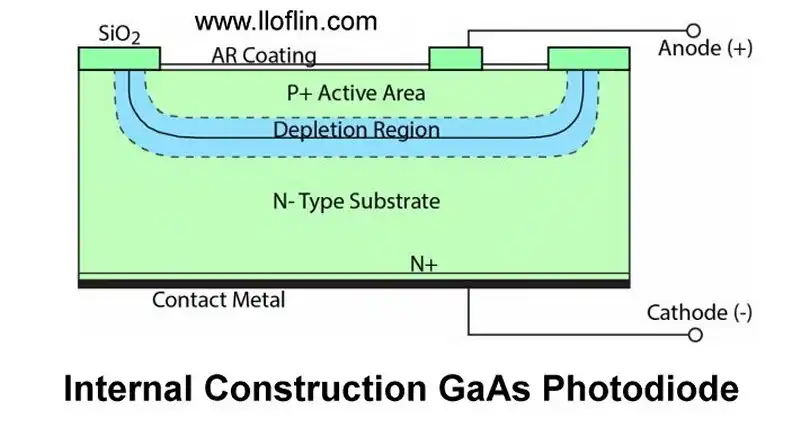
Gallium-arsenide photodiode internal diagram.
Gallium Arsenide (GaAs) photodiodes convert light into electrical current, driven by electron flow from negative to positive, as in my electron flow model. This page reviews their operation, historical context, and related topics like ferrites and SCRs, building on my selenium and cesium discussions.
GaAs Photodiode Operation
A GaAs (Gallium Arsenide) photodiode operates on the principle of converting light into electrical current. When photons (light particles) strike the GaAs semiconductor material, they are absorbed if their energy is greater than the bandgap energy of GaAs. The bandgap energy of GaAs is approximately 1.43 eV, corresponding to light with a wavelength shorter than about 870 nm.
The color associated with a wavelength of 870 nm is infrared. This wavelength falls outside the visible spectrum, which ranges from approximately 400 nm (violet) to 700 nm (red). Infrared light is not visible to the human eye but can be detected by specialized equipment like night vision devices or certain types of cameras.
Photogeneration of Electron-Hole Pairs: The absorbed photons excite electrons from the valence band to the conduction band, creating electron-hole pairs. This process is known as photogeneration in semiconductors.
Separation of Charge Carriers: GaAs photodiodes are typically structured as p-n junctions. In photovoltaic mode (no external bias), the built-in electric field at the junction separates the photogenerated electrons and holes. Electrons move towards the n-type region (cathode), while holes move towards the p-type region (anode).
Photovoltaic Mode: The open-circuit voltage of a GaAs photodiode is typically ~0.8–1.0 V, and the short-circuit current varies, often <200 µA for small devices under low light. This creates a potential difference between the terminals. Electrons can’t migrate back across the p-n junction but flow through an external circuit from n-type (cathode) to p-type (anode), transferring energy to the load.
Photoconductive Mode: In reverse-biased conditions, the electric field enhances separation, increasing response speed but requiring external power. The photocurrent is proportional to the intensity of the incident light.
Electron Flow: Electrons are the only charges moving in the physical sense. The movement of "holes" is a construct, not a real event involving physical matter, aligning with my electron flow model.
Dark Current: Even without light, a small current (dark current) occurs due to thermal generation of carriers. GaAs photodiodes minimize this, often using cooling for high-sensitivity applications, enhancing signal-to-noise ratio.
Table of semiconductor bandgaps:
| Material | Bandgap (eV) |
|---|---|
| GaAs | 1.43 |
| Silicon | 1.12 |
| Selenium | 1.8–2.0 |
| CIGS | 1.0–1.7 |
Key Features of GaAs Photodiodes
High Responsivity: GaAs has a high absorption coefficient for infrared light (~10⁴ cm⁻¹ at 850 nm), making these photodiodes very responsive to light in the 400–900 nm range, peaking at ~850 nm.
Fast Response: Due to the high electron mobility in GaAs (~8500 cm²/V·s vs. silicon’s ~1500 cm²/V·s), these photodiodes have fast response times, beneficial for high-speed optical communication, LiDAR, and fiber optics.
Low Noise: When properly designed, GaAs photodiodes offer low noise performance, crucial for sensitive detection applications, enhanced by their wide bandgap.
History of GaAs
From Wafer World:
In 1955, scientists were able to grow a single crystal of GaAs and use it for building photocells.
In 1965, Carver Mead fabricated and tested the first GaAs-based field-effect transistor (MESFET).
During the 1970s and 1980s, GaAs was used to build a wide range of circuits for everything from high-end computers to cell phones.
By the 1970s, GaAs MESFETs were developed as three-terminal devices with a gate length of 1 µm, and found applications in microwave amplification.
In the 1990s, these GaAs MESFETs made their first major impact on the commercial wireless market.
In 1992, a new class of LEDs using GaAs material was introduced. Known as resonant-cavity light-emitting diodes (RCLED), these devices provided increased emission intensities parallel to the cavity's optical axis, enabling higher coupling efficiencies to optical fibers.
I used MESFETs in the 1980–90s in the satellite TV industry. Further:
Today, GaAs is known to be one of the most powerful semiconductors. Its higher electron saturation velocity allows better electron mobility, which makes it a great material to use when creating higher-frequency devices. It also produces lesser noise and can operate in higher power levels compared to silicon. These characteristics make GaAs reclaim wafers a good material to use in the manufacturing of devices such as cellular phones and technological advancements in satellite communications and radar systems.
As of 2025, GaAs is critical in 5G networks, multi-junction solar cells (~30% efficiency), and advanced radar systems, as explored in my selenium photovoltaics.
Ferrite Materials
Lewis: When were ferrite materials invented?
Answer: The first practical application of ferrites came about with the work of Dr. Yogoro Kato and Dr. Takeshi Takei in Japan in 1930. However, it was in the 1940s and 1950s that ferrites became widely used, particularly in electronics and telecommunications, due to research at Philips by J.L. Snoek and others.
Ferrite materials are ceramic compounds consisting primarily of iron oxide (Fe₂O₃ or Fe₃O₄) combined with one or more additional metallic elements like manganese, zinc, nickel, or magnesium. Here are some common types of ferrites based on their composition:
Manganese-Zinc (MnZn) Ferrites: These are made from iron oxide with manganese and zinc. They are used in applications where low core losses are required at high frequencies, such as transformers.
Nickel-Zinc (NiZn) Ferrites: Composed of iron oxide along with nickel and zinc. They are known for their higher resistivity, suitable for higher frequency applications like antennas.
Magnesium-Zinc (MgZn) Ferrites: These include magnesium and zinc with iron oxide, often used in TV applications and transformers.
Barium and Strontium Ferrites: Typically used to make permanent magnets, with a hexagonal crystal structure.
Cobalt Ferrites: Used in magnetic recording due to their strong magnetic properties.
The exact composition can vary, altering the material's magnetic, electrical, and physical properties, making different ferrites suitable for applications like EMI suppression, wireless charging, and microwave components, as in my chemistry for electronics.
Miscellaneous Subjects
Unijunction Transistor (UJT):
The unijunction transistor (UJT) was invented in 1953 by General Electric. Its primary application was in oscillator circuits and timing applications due to its stable negative resistance region. UJTs are now niche, replaced by integrated circuits in most applications.
Silicon Controlled Rectifier (SCR):
The Silicon Controlled Rectifier (SCR), or thyristor, was developed by General Electric and announced in 1957. It revolutionized power electronics, enabling control of high power with a small triggering signal. Modern uses include motor drives and renewable energy inverters.
Neon Sign Power Supply:
Neon signs typically operate on AC (alternating current) due to high-voltage transformers (~2–15 kV), which are efficient for gas discharge and electrode longevity. Modern LED neon signs use DC power supplies for efficiency.
Gases in Neon Signs:
Neon: Produces reddish-orange light.
Argon: Pale blue or lavender, often with mercury for bright blue or phosphor-coated colors (white, pink, green).
Helium: Pink to reddish, used in cold climates.
Krypton: Whiteish or pale yellow, less common.
Xenon: Blue or lavender, used for white light with phosphors.
Mercury Vapor: Produces UV to excite phosphors for various colors.
Environmental concerns have led to mercury-free phosphors in modern signs, aligning with my training program.
Conclusion
GaAs photodiodes, driven by electron flow from negative to positive, exemplify semiconductor advancements, as in my electron flow model. From early photocells to 5G and solar applications, GaAs remains vital, alongside ferrites and SCRs in modern electronics. Explore my training program, circuit projects, or YouTube videos.
Share This Article
References
Paul Sharz, Practical Electronics for Inventors, McGraw-Hill Education.
Stephen L. Herman, Electric Circuits, Delmar Cengage Learning.
Personal correspondence with xAI, 2025.
Lewis Loflin’s teaching materials, Bristol Community College, 1980s–1990s.
Wafer World, GaAs History, accessed 2025.
Related Subjects
- Chemistry for Electronics:
- Why Chemistry is Useful for Learning Electronics
- Electrochemistry and Battery Charger Chemistry
- What is Electrochlorination and Electrolysis?
- Electroplating One Gram of Copper Working Example
- TL431 Battery Charger Voltage Detector Circuits Schematics
- TL431 Sink Mode Constant Current Circuits
- Physics and Chemistry for Electronics:
- Cesium Photo Detectors, Zinc Photocells, and Bandgap Explained
- Cesium Photoelectric Cells
- Is Zinc Photovoltaic?
- Bandgap versus Work Function Key Differences
- How Selenium Rectifiers and Photocells Operate
- Brief Overview of Vacuum Tubes and Circuits
- Basic Review Operation GaAs Photodiodes
- Electronics Education and Careers Defined Six Parts:
- Applied versus Theoretical Science Relation to Electronics
- How does applied science differ from theoretical science?
- Is electronics an applied science?
- What is the difference between electronics and electrical technicians?
- What does "academic ability" really mean in practical terms?
- How does an electronics technician differ from an engineer?
- Electronic Circuits and Applications:
- Electronics and Technology Built at Home Mainpage
- Arduino Constant Current H-Bridge Motor Control
- LM555 Timer Monostable AC Power Phase Control Demo