Introduction
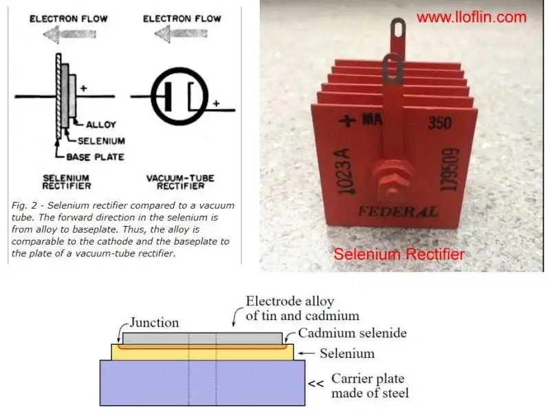
Various selenium rectifiers. Many were stacks of individual selenium diodes in series.
Selenium rectifiers and photovoltaic cells were pivotal in early electronics, leveraging electron flow from negative to positive, as in my electron flow model. This page explores selenium’s semiconductor properties and modern CIS/CIGS solar cells, building on my cesium photocell discussion.
See What is a CIS Solar Cell? below.
Selenium Rectifiers
The selenium rectifier consists of a metal base plate (usually iron or aluminum), a selenium layer, and a metal cap or electrode. The base plate acts as the cathode (negative terminal), and the metal cap as the anode (positive terminal). Electrons flow from the cathode to the anode through an external load, facilitated by the selenium-metal junction.
This setup leverages the rectifying characteristics of the selenium-metal junction, allowing current to flow predominantly in one direction. The Schottky barrier, formed by the work function difference between the metal (~4.2 eV for aluminum) and selenium (~4.8–5.0 eV), drives this rectification, aligning with my semiconductor model.
Selenium rectifiers were widely used until the 1970s, when silicon diodes, with higher efficiency and durability, replaced them.
Electrical Properties of Selenium
Selenium, as a semiconductor, exhibits several notable electrical properties.
Selenium is a p-type semiconductor with excess positive charge carriers (holes). This property is due to the presence of acceptor impurities, which create vacancies in the valence band.
Selenium can be doped with various elements to modify its electrical properties. For instance, doping with arsenic can turn it into an n-type semiconductor, altering its conductivity and behavior in electronic devices.
Like many semiconductors, selenium's electrical conductivity increases with temperature. This is because thermal energy can free more electrons from covalent bonds.
Selenium rectifiers, which were once commonly used before the advent of silicon diodes, leverage their ability to conduct electricity preferentially in one direction. This rectification property is due to the formation of a Schottky barrier at the metal-selenium interface.
A Schottky barrier (a Schottky diode or rectifying contact) is a potential energy barrier for electrons formed at a metal-semiconductor junction. This barrier arises from the difference in work functions between metal and semiconductors.
The work function indicates how easy or hard it is to dislodge an electron from the surface of a material. A lower work function means electrons are more easily removed, while a higher work function means they are more tightly bound to the material. This difference between the selenium semiconductor and the metal plate creates an imbalance of electrons and, thus, voltage or rectification.
Because electrons can more easily leave the metal due to its lower work function, they flow towards the selenium (which has a higher work function) through an external load. This sets up the conditions for the Schottky barrier and gives rise to the junction's rectifying properties.
Selenium's resistivity can vary widely depending on its form and purity. Resistivity (ρ) is an intrinsic property, calculated as ρ = R·A/L (ohm·meters), where R is resistance, A is cross-sectional area, and L is length. Metals like copper have low resistivity, while insulators like rubber have high resistivity. Like most semiconductors, selenium is in between, and its resistivity (~10⁴–10⁶ Ω·cm for amorphous form) can be manipulated through doping, temperature changes, or light exposure.
Selenium’s photoconductivity, where conductivity increases under light due to electron-hole pair generation, ties to its bandgap, as discussed in my bandgap analysis.
Selenium Photovoltaic Cells

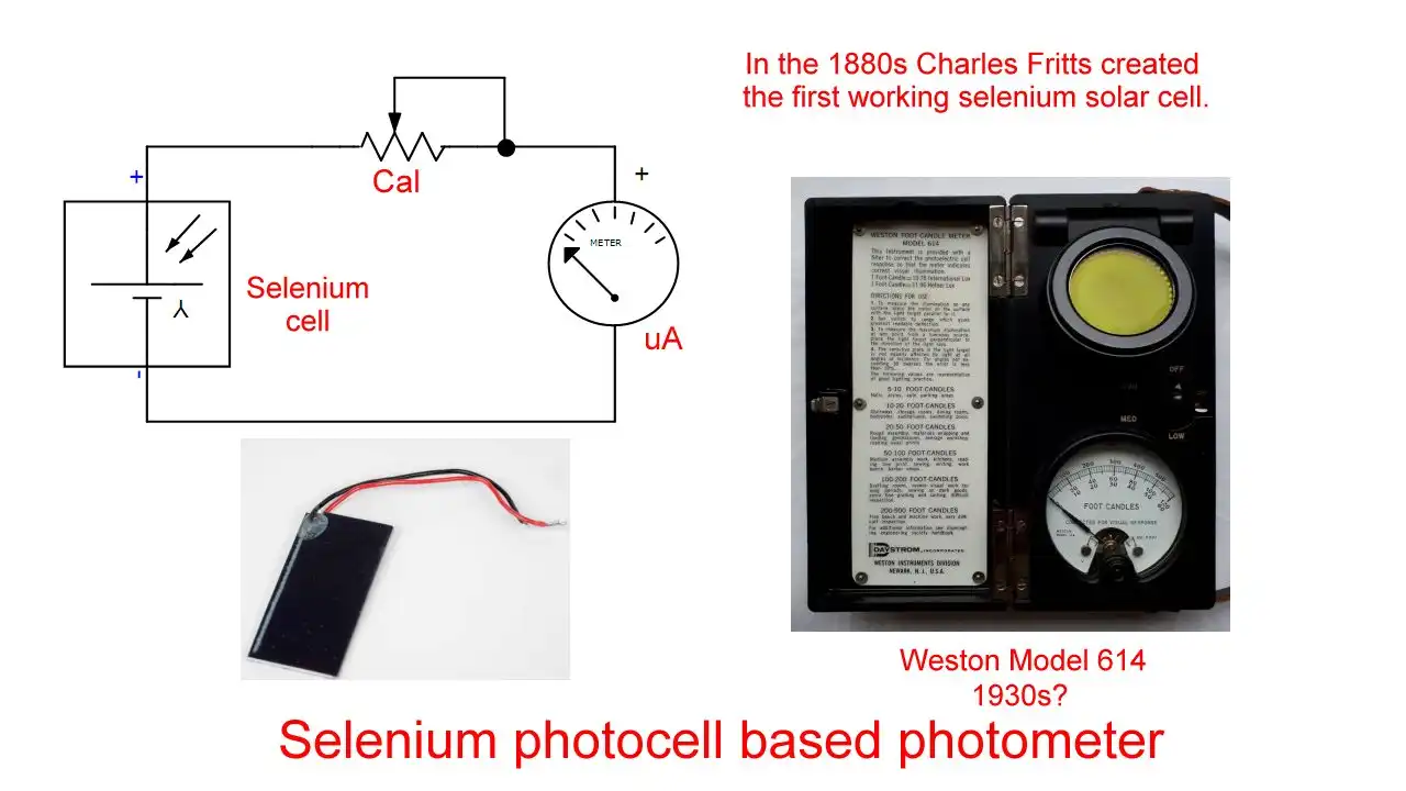
Selenium solar cell used as a photometer.
Click for a larger image.
Selenium photovoltaic cells are photoelectric devices that generate or control electric currents. They are used in various applications, including photographic exposure meters, burglar alarms, electronic door opening and counting devices, electronic control systems in factory assembly lines, and industrial color perceptors.
Selenium was one of the first materials discovered to have photovoltaic properties. In 1873, its photoconductivity was found, leading to early experiments with selenium-based solar cells by the 1880s, among the first solid-state solar cells created.
Selenium was the world's first solid-state solar cell and initiated contemporary photovoltaic research. However, the efficiency of selenium photovoltaics is limited to ~5–6.5% in niche applications, now largely obsolete for mainstream solar due to silicon’s superior efficiency (~15–25%).
Selenium is highly photoconductive, meaning its electrical conductivity increases when exposed to light. When photons strike the selenium, they excite electrons, creating more free-charge carriers, thus increasing conductivity.

Vintage selenium solar cells.
Selenium's amorphous form has a band gap of approximately 1.95 eV, influencing its electrical behavior. These properties make selenium helpful in various applications, although many have been superseded by silicon and other materials due to performance and efficiency reasons. Selenium's unique properties still find niche uses, especially in photoconductive applications.
Selenium has a relatively wide bandgap (approximately 1.95 eV), which is advantageous for specific photovoltaic applications. It can be used with materials with different bandgaps to capture a broader spectrum of sunlight. The bandgap determines the wavelength of light that a semiconductor can absorb or emit. For instance, materials with a smaller bandgap might be used for infrared detectors, while those with a larger bandgap might work with visible or UV light.
The bandgap of a solar cell's material influences how much solar energy can be absorbed. Different bandgap materials can be stacked in multi-junction cells to capture a broader spectrum of sunlight.
Research has shown that selenium solar cells can achieve open-circuit voltages of ~0.8–0.9 V, compared to silicon’s ~0.5–0.75 V, indicating potential for niche applications. Despite their photovoltaic properties, pure selenium solar cells have historically suffered from low efficiency. Interest in selenium for photovoltaics persists due to its potential in multi-junction cells or as part of more complex semiconductor alloys designed to optimize light absorption and conversion efficiency.
While selenium isn't the leading material in today's commercial solar market, its photovoltaic properties are well-recognized. It is relevant in research and development to advance solar cell technology, particularly in specialized applications like thin-film technologies, as seen in my chemistry for electronics.
Selenium’s early role paved the way for modern thin-film technologies like CIS/CIGS, discussed below.
What is a CIS Solar Cell?
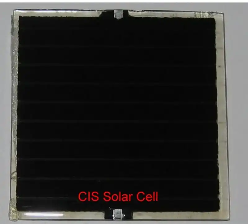
Copper Indium Selenide Solar Cell
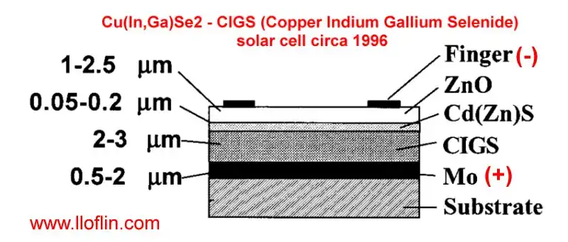
CIS stands for Copper Indium Selenide (CuInSe₂). When gallium is added to the mix, it's known as CIGS (Cu(In,Ga)Se₂). The addition of gallium increases the bandgap of the material (from ~1.0 eV for CIS to ~1.0–1.7 eV for CIGS), which can lead to higher efficiency. They've shown potential for high conversion efficiencies, with some lab-scale CIGS cells achieving efficiencies over 23% as of 2025.
While not as common as silicon in the solar industry, selenium is used in combination with other elements in some types of thin-film solar cells. One notable example is Copper Indium Gallium Selenide (CIGS) solar cells. CIGS cells use a compound semiconductor made of copper, indium, gallium, and selenium, which has a high absorption coefficient for solar radiation, making it efficient for thin-film applications.
While a Schottky barrier may be present due to contact with a metal back, CIS cells don't rely on Schottky barriers. The primary operation is based on the p-n junction or heterojunction formed within the device.
Manufacturing at scale while keeping costs down has been a challenge, though progress has been made. Besides traditional solar panels, CIS/CIGS technology is explored for use in building-integrated photovoltaics (BIPV), portable electronics, flexible panels, and space applications due to their radiation resistance and lightweight design.
The scarcity of indium and gallium compared to silicon is a concern for large-scale production, scalability, and cost.
Selenium is an element related to sulfur producing pungent, toxic gas if burned, often identified as selenium dioxide (SeO₂). This gas has a characteristic odor, somewhat reminiscent of horseradish, garlic, or decaying matter, and it's highly irritating to the respiratory system, eyes, and skin. Handle selenium with ventilation and protective equipment to avoid exposure.
P-n junctions in CIS/CIGS cells drive electron flow, as in my semiconductor discussion.
Bandgaps of key photovoltaic materials:
| Material | Bandgap (eV) |
|---|---|
| Selenium | 1.8–2.0 |
| Silicon | 1.12 |
| CIS | ~1.0 |
| CIGS | 1.0–1.7 |
Addendum: CIS/CIGS Structure
Layers deposited on CIGS solar cell.
In the context of a CIS (Copper Indium Selenide) solar cell, Mo refers to Molybdenum. Molybdenum is commonly used as the back contact material in CIS solar cells.
Molybdenum (Mo) acts as a back electrode (+) or contact layer. Provides good electrical conductivity and adhesion to the substrate (usually glass). Offers high temperature stability, which is crucial during the high-temperature deposition processes of the CIS absorber layer. Helps in preventing diffusion of contaminants from the substrate into the active layers of the solar cell. This layer is typically deposited via sputtering onto the substrate before the deposition of the CIS absorber layer.
Cu(In,Ga)Se2, also known as CIGS (Copper Indium Gallium Selenide), is similar to CIS but includes Gallium, which modifies some of its properties.
Molybdenum (Mo): Just like in CIS cells, Molybdenum serves as the back contact in CIGS solar cells is the Positive Terminal (+). The back contact is where holes are collected.
The Cd(Zn)S layer acts as a buffer layer between the CIGS absorber and the front TCO (Transparent Conductive Oxide) contact. The Cd(Zn)S layer has a wider bandgap (around 2.4 eV for CdS and adjustable with Zn content) compared to CIGS (1.1–1.5 eV), allowing shorter wavelength light to pass through to the CIGS layer while absorbing less light itself. This enhances the overall light absorption in the CIGS layer. When properly doped, it can provide a pathway for electrons while maintaining low resistance.
Negative Terminal (-): The front contact, typically a transparent conductive oxide like ZnO or ITO, where electrons are collected.
For CIGS solar cells, the open-circuit voltage typically ranges from about 0.6 to 0.9 volts. The incorporation of Gallium increases the bandgap, generally leading to a higher open-circuit voltage (Voc) compared to pure CIS cells.
Maximum Power Point Voltage (Vmp): This is slightly lower than Voc, usually around 0.5 to 0.7 volts under standard test conditions. The addition of Gallium in CIGS allows for better tunability of the bandgap, which can enhance both voltage and efficiency compared to CIS.
The manufacturing of CIGS photocells is energy-intensive, particularly due to the deposition processes. However, advancements in deposition techniques, material efficiency, and scale of production can significantly influence the overall energy intensity.
Energy Payback Time (EPBT): For CIGS modules, this has been reported to be around 1 to 2 years under European conditions, which indicates the amount of time it takes for the module to produce energy equivalent to that used in its production. This can be compared to silicon modules, which might have an EPBT of 1.5 to 3 years or more, depending on technology and location.
Conclusion
Selenium’s legacy in rectifiers and early photovoltaic cells laid the foundation for modern semiconductors, now advanced by CIS/CIGS technologies. Electron flow from negative to positive, as in my electron flow model, drives these devices. While selenium is niche today, CIGS cells thrive in flexible and space applications. Explore my training program, circuit projects, or YouTube videos.
Share This Article
References
Paul Sharz, Practical Electronics for Inventors, McGraw-Hill Education.
Stephen L. Herman, Electric Circuits, Delmar Cengage Learning.
Personal correspondence with xAI, 2025.
Lewis Loflin’s teaching materials, Bristol Community College, 1980s–1990s.
National Renewable Energy Laboratory, CIGS Solar Cell Data, accessed 2025.
Related Subjects
- Chemistry for Electronics:
- Why Chemistry is Useful for Learning Electronics
- Electrochemistry and Battery Charger Chemistry
- What is Electrochlorination and Electrolysis?
- Electroplating One Gram of Copper Working Example
- TL431 Battery Charger Voltage Detector Circuits Schematics
- TL431 Sink Mode Constant Current Circuits
- Physics and Chemistry for Electronics:
- Cesium Photo Detectors, Zinc Photocells, and Bandgap Explained
- Cesium Photoelectric Cells
- Is Zinc Photovoltaic?
- Bandgap versus Work Function Key Differences
- How Selenium Rectifiers and Photocells Operate
- Brief Overview of Vacuum Tubes and Circuits
- Basic Review Operation GaAs Photodiodes
- Electronics Education and Careers Defined Six Parts:
- Applied versus Theoretical Science Relation to Electronics
- How does applied science differ from theoretical science?
- Is electronics an applied science?
- What is the difference between electronics and electrical technicians?
- What does "academic ability" really mean in practical terms?
- How does an electronics technician differ from an engineer?
- Electronic Circuits and Applications:
- Electronics and Technology Built at Home Mainpage
- Arduino Constant Current H-Bridge Motor Control
- LM555 Timer Monostable AC Power Phase Control Demo