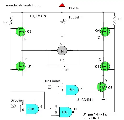
H-bridge schematic with speed control.
Figure 1: H-bridge control circuit with enable and direction pins.

Power MOSFET H-Bridge Circuit Examples

by Lewis Loflin (lloflin2@gmail.com)

Circuit Overview

This article explores variations on the Power MOSFET H-bridge. The design presented here incorporates dedicated Enable and Direction pins, allowing for seamless integration with microcontroller systems. The enable functionality is particularly useful for implementing Pulse Width Modulation (PWM) to control motor speed.

Operational Logic

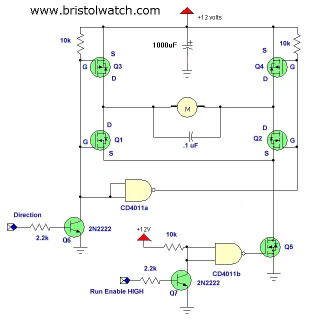
The circuit utilizes a CD4011B quad NAND gate as an inverter for logic control:

  • Enable Functionality: A 'HIGH' signal on the enable pin activates transistor Q7, driving its collector 'LOW'. This signal, processed through the CD4011B (acting as an inverter), produces a 'HIGH' output on the gate of Q5, activating the MOSFET and powering the motor.
  • Directional Control:
    • LOW (0V): With the Direction pin at LOW, Q6 remains off, driving its collector 'HIGH'. This triggers Q1 and, via the CD4011, Q4. Current flows through the motor path formed by Q1 and Q4.
    • HIGH (5V): The Direction pin turns Q6 'ON', pulling its collector 'LOW'. This switches off Q1 and Q4 and activates Q2 and Q3, reversing the current path through the motor.

Design Considerations

This design is optimized for 5V microprocessor interfacing. Note that the operating voltage for the logic section is limited to 15V by the CD4011B. When selecting power components, verify that the supply voltage (Vcc) does not exceed the Vgs limits of your chosen MOSFETs (typically 20V for the devices listed below).

Parts List

  • Q1, Q2, Q5: IRF630 (N-Channel MOSFET)
  • Q3, Q4: IRF9630 (P-Channel MOSFET)

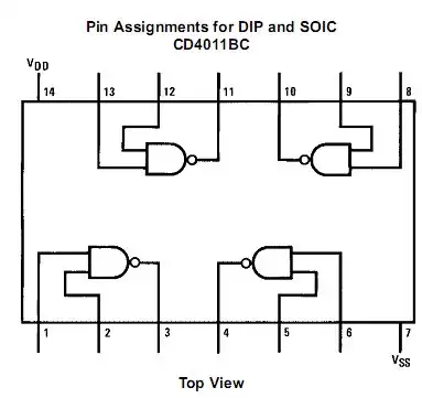
CD4011 pin connections
Figure 2: CD4011 Pin Connections.

Using MOSFETs for H-bridge
Figure 3: Alternative H-bridge MOSFET Configuration.
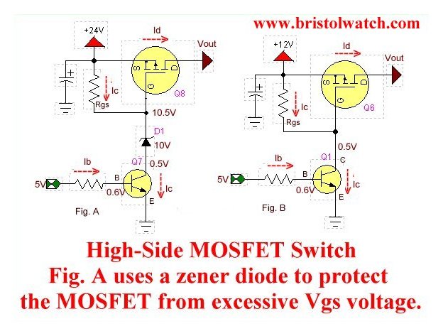
P-channel Power MOSFET Switch
Figure 4: P-channel Power MOSFET used for Vcc high-side switching.

The circuit in Figure 4 can be used to cut Vcc on/off or serve as a high-side switch for PWM speed control.

Additional Resources & Related Circuits

About the Author

Lewis Loflin is an independent researcher and educator from Bristol, Virginia. He has been trained in and worked with electronics since the 1970s. He has studied physics, chemistry, and related sciences since the 1970s and in college. He became proficient in both through decades of self-teaching, experimentation, and applied projects. His work emphasizes verifiable physical principles, practical experimentation, and critical evaluation of scientific claims.

Lewis has built hundreds of educational projects in applied electronics, microcontrollers, and general science. His website, Bristolwatch.com, presents this work as a modern “hands-on science lab,” encouraging readers to build, measure, and understand how the natural world and electronic systems truly operate.

With extensive experience servicing and studying vintage televisions and vacuum-tube electronics since the 1970s, Lewis possesses first-hand knowledge of components such as selenium high-voltage rectifiers, CRT circuits, and flyback transformers—knowledge often absent from modern literature. His detailed analyses frequently correct misconceptions about these technologies, particularly in high-frequency horizontal-deflection and high-voltage rectifier applications.

Lewis continues to use the electron-flow model when describing circuits and devices. This reflects the actual physical direction of charge movement in vacuum tubes, semiconductors, and gas-discharge devices, and avoids the conceptual confusion introduced by the older "positive-flow" convention. Understanding electron flow is essential for explaining how these devices truly function at the physical level.

While Gemini AI has been used for writing assistance and discussion support, all technical material is independently verified through direct experimentation, testing, and comparison with official datasheets and reference sources.

Support This Site – Donate via PayPal