Toggle ON-OFF LED on RB1 Based on External Interrupt on RB0
by Lewis Loflin
Follow @Lewis90068157
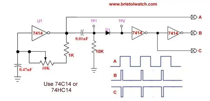
SN74HC14 based square wave generator with differentiator circuit.
The next section requires a square wave generator or source. This used the above setup one can build. See Simple Schmitt Trigger SN74HC14 Square Wave Generator
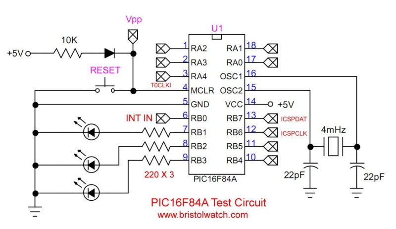
Connect either A or B to RB0 INT pin 6 on the PIC16F84A. With a frequency counter (a function on better digital volt meters) measure the input frequency. The LED will blink at half the input frequency.
;=================================================================================
;   CLOCK: External 4MHz (instruction execution time: 1usec)
;	Program name: PORTB RB0 External Interrupts.
;	Toggle ON-OFF LED on RB1 Based on External Interrupt on RB0
;	Date: 6/22/2024
;	Author: Lewis Loflin
;	LEDS connected to GRD RB1-RB3. Switch, pulse inputs RA0-RA2
;======================================================================

	; Check assembler divice settings!
 	list      p=16F84A      ; list directive to define processor
	#include <p16F84A.inc>  ; processor specific variable definitions
	errorlevel  -302        ; Ignore error message when storing to Bank 1.

  	__CONFIG        _CP_OFF & _PWRTE_ON & _WDT_OFF & _XT_OSC

;======================================================================

; define

LED1 EQU 1
LED2 EQU 2
LED3 EQU 3

; Assign each register from Bank 0 RAM.
; range 0xC0-0x4F
CBLOCK  0xC0
B0
B1
B2
temp1
temp2
CNT1
CNT2
CNT3
CNT4
ENDC ; Conclude Bank 0 RAM assignments.

;*******************************************
	ORG     0x000
	goto    setup

	ORG     0x004
	; isr code can go here
		;	incf CNT1
	movlw 0x02
	xorwf PORTB, f
	bcf INTCON, INTF ; clear RB0/INT Flag bit
	retfie    ; return from interrupt

;********************************************


setup

    BSF	STATUS,RP0   ;Jump to bank 1
	; BANKSEL TRISA
	; 1 = INPUT, 0 = OUTPUT
	MOVLW	B'00010000'		;Config Port A, RA0 to RA3 are outputs
	MOVWF	TRISA			;Set I/O configuration for PORTA
	MOVLW	B'11110001'		;Config Port B, RB1-3 OUTPUT, RB0, RB4-7 INPUT
	MOVWF	TRISB			;Set I/O configuration for PORTB

	; OPTION_REG bit 6 INTEDG: Interrupt Edge Select bit
	; 1 = Interrupt on rising edge of RB0/INT pin
	; 0 = Interrupt on falling edge of RB0/INT pin
	BSF OPTION_REG, 6 ; LOW to HIGH

	BCF	STATUS,RP0		    ;Jump back to bank 0 of PIC.
	; BANKSEL INTCON


	CLRF	PORTA			;Clear all I/O's of PORTA
	CLRF	PORTB
				;Clear all I/O's of PORTB
	CLRF INTCON
	BSF INTCON, 7 ; GIE  enable global INT
	BSF INTCON, 4 ; INTE RB0/INT External Interrupt Enable bit
	BCF INTCON, 1 ; INTF ; RB0/INT External Interrupt Flag bit
	; INTF must be cleared in software

goto main

main
; do nothing
goto main

end
- Operate PIC16F84A TMR0 from RA4/T0CKI Pulse Input
- PIC16F84A-PIC16F628A Pull Up Resistors with Interrupts
- Programming PIC16F84A-PIC16f628a Timers by Example
- Programming PIC16F84A-PIC16F628A TMR0 Interrupts
- Programming PIC16F84A Software Delay Routines by Example
- YouTube videos:
- PIC16F84A-628A Hardware Time Delays
- PIC16F84A-628A Timer Interrupt Delays
- PIC16F84A-628A Pullups and Interrupts
- PIC16F84A-628A Hardware Interrupts Tutorial
- Microchip PIC related videos:
- How to Use K150 PIC Programmer
- Microchip PIC16F628A Basic H-Bridge Motor Control
- Microchip PIC16F628A Counts BCD on 8 LEDs
- PIC16F84A Operates H-Bridge Motor Control
- PIC16F84A Operates MOSFET H-Bridge
- Using Velleman K8048 PIC Development Board
- Arduino Port Registers Revisited
- Digispark ATtiny85 with MCP23016 GPIO Expander
- Safely Build Program a H-Bridge
- Build H-Bridge Motor Control Without Fireworks
- MOSFET H-Bridge for Arduino 2
- Microchip PIC16F84A H-Bridge Motor Control
- Microchip PIC16F628A Basic H-Bridge Motor Control
- PICAXE Operates H-Bridge Motor Controller
- PICAXE Microcontroller Controls Motor Speed - Direction
- PICAXE Projects
Web site Copyright Lewis Loflin, All rights reserved.
If using this material on another site, please provide a link back to my site.