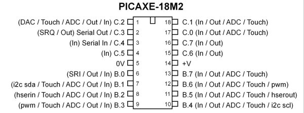
Fig. 1 PICAXE 18M2.
74HC595 Shift Register and PICAXE 18M2 Microcontroller
This is very similar to the earlier demo using to 74HC165 with one important difference in that the 74HC595 has an internal 8-bit latch. The output to the LEDs remains stable until new data is "latched" by the PICAXE micro-controller. This provides a smoother and flicker-free output than the 74HC164. For more information see Using the 74HC165 Shift Register with the PICAXE Micro-Controller.
Using a row of eight LEDs the circuit will count in binary (right to left) 0 to 255. To see a wiring diagram of the board I built and used in the demo see Exploring the PICAXE Micro-Controller.
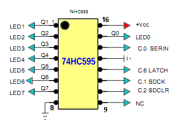
Fig. 2
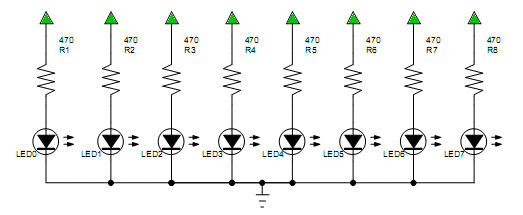
Fig. 3
Fig. 2 above shows the pinout and connections to the PICAXE micro-controller and the eight LEDs of Fig. 3 which is a common cathode configuration. Pin connections are as follows:
SER (pin 14) is for data bit input. Connect to pin 17 (C.0) on PICAXE.
SDCK (pin 11) data clock. Connect to pin 18 (C.1) on PICAXE
SDCLR (pin 10) clear data register. Connect to pin 1 (C.2) on PICAXE. Could be connected to +5 volts.
LATCH (pin 12 RCK) a HIGH transfers SR data to latch. Connect to pin 15 (C.6) on PICAXE.
ENABLE output enable (pin 13 or G-NOT) a low outputs the latch data. Connect to pin 16 (C.7) on PICAXE. Could be connected to ground.
The 74H565 consists of three main sections: 8-bit shift register, 8-bit latch, 8-bit output enable.
This device contains an 8-bit serial-in, parallel-out shift register that feeds an 8-bit D-type storage register. The storage register has 8 3-STATE outputs. Separate clocks are provided for both the shift register and the 8-bit storage register.
The shift register has a direct-overriding clear, serial input, and serial output (standard) pins for cascading. Both the shift register and storage register use positive-edge triggered clocks. If both clocks are connected together, the shift register state will always be one clock pulse ahead of the storage register.
The Program Code
#picaxe 18m2 ; type chip used
; set internal clock to 4 mHz
setfreq m4  ; All M2 partsinternalk31,
; k250, k500, m1, m2, m4, m8,m16,m32


symbol SER = C.0
; SER (pin 14) is for data bit to SR.
symbol SDCK = C.1
; SDCK (pin 11) data clock
symbol SDCLR = C.2
; SDCLR (pin 10) clear data register on LOW.
symbol LATCH = C.6
; LATCH  (pin 12 RCK) HIGH latches SR data
symbol ENABLE= C.7
; ENABLE output for latch data (pin 13 or G-NOT)

; user variables
symbol val = b0
symbol temp1 = b1
symbol j =b2
symbol i = b3

LOW ENABLE
HIGH SDCLR


main:


   for j = 0 to 255
     val = j
     for i = 1 to 8
        temp1 = val & %00000001
        if temp1 = 1 then HIGH SER
        else LOW SER
        endif
        pulsout SDCK,1
        val = val / 2 ; shift bits one place right
     next i

     pulsout LATCH,1
     ; data retained until next cycle
     pause 400
   next j


goto main
Picaxe Micro-controller Projects!
The PICAXE series of micro-controllers rank as the easiest and most cost effective way to use Microchip processors. I wanted an easier and less expensive way to introduce my students to the "PIC" micro-controller. Here I hope to get those starting out past poorly written literature and lack of simple working code examples.
- PICAXE Related videos Oct. 2016:
- Tutorial: Programming-Using PICAXE-18M2 Microcontroller
- How to setup PICAXE Pulse Width Modulation
- PICAXE TA8050P H-Bridge with Motor Control
- PICAXE TA8050P H-Bridge with Motor Speed Control
- PICAXE-18M2 Operates MOSFET H-Bridge
- PICAXE-18M2 Uses MCP23016 GPIO Expander
- Solar Panel Charge Controller Using PICAXE Microcontroller
- Exploring the PICAXE Micro-Controller
- Understanding Micro-Controller Input/Output Ports
- Using the 74HC165 Shift Register with the PICAXE Micro-Controller
- Connecting the 74HC595 Shift Register to PICAXE Micro-controller
- Using 7-Segment Displays with the PICAXE Micro-Controller
- Potentiometers and Analog-to-Digital Conversion with the PICAXE
- Pulse-Width Modulation Motor Speed Control and the PICAXE Micro-Controller
- Connecting the PICAXE to the DS1307 Real Time Clock
- Connecting the PICAXE to an External EEPROM (24LC08)
- Connecting a Servo to a PICAXE
- Connecting the TLC548 to the PICAXE
- Connecting the Ad5220 Digital Potentiometer to the PICAXE
See How I got into Electronics
