
Fig. 1
Click for larger view.
Power TL431 Constant Current Source
by Lewis Loflin
See YouTube video TL431 Power Constant Current Source Demo 1
The goal of this tutorial is the teach circuit theory. This is also an inexpensive way of creating a constant current source for circuit prototyping.
This tutorial explores how power divides in a series circuits. This also explores using power transistors to boost current output from a basic TL431 constant current source circuit.
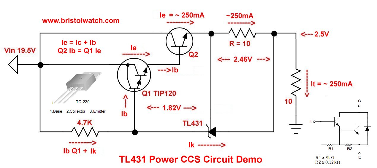
Fig. 1 is the TL431 power constant current source schematic.
A 10-Ohm resistor R set the series current by controlling the bias current through the Q1 and Q2 base-emitter-base-emitter circuit. Q1's emitter current (Ie) is the base current for Q2.
These three PN junction drop ~1.8V.
The Q2 emitter current (Ie) minus a few milliamps Ik in the TL431 is most of the circuit current. Ik is disregarded in the following example.
The R voltage is rounded off to 5V.
The series current I is fixed by R (10-Ohms) with the formula 2.5V / R = 2.5V / 10 = 250mA.

Fig. 2 TL431 constant current source test setup for 250mA.

Fig. 3
TL431 constant current source test setup for 250mA with a Vin of 19.5V. The current I is set by a 10-Ohm resistor R.
The sum of all power drops will add back the Vin input power.
The input voltage Vin divides mainly across the Q2 pass transistor, the 10-Ohm current set resistor R, and the output load. The total power input is 19.V * 250mA = 4.874W.
Q2 voltage drop is 14.5V with a current of 250mA. The transistor dissipates 3.625W.
Current set resistor R always drops ~2.5V * 250mA = 625mW. The 10-Ohm load resistor is identical at 2.5V at 625mW.
~75% of the power is wasted across Q2.

Fig. 4
The circuit in Fig. 4 is identical to Fig. 3, except the input voltage is 8V. The overall power input from Vin is 2W.
R and load are fixed, the power dissipation in Q2 drops 750mW or 37.5% of the Vin power.
In summary excess power is dissipated across Q2. Reducing the input voltage to just above the required voltage (Vload + VR + 3V) reduces wasted power.

Fig. 5
Fig. 5 is heavier current test setup. R is changed to 2-Ohms for a current of 1.25A. The load resistance is now 5-Ohms.
The output voltage on the load is 6.25V at ~7.8W.
The R voltage is still ~2.5V at 1.25A for 3.125W
The Q2 collector-emitter voltage drop is 10.75V at 13.45W with a Vin of 19.5V.

Fig. 6
Fig. 6 is identical to Fig. 5 except the input voltage is 15V. This reduced the Q2 collector-emitter voltage 6.25V at 7.825W.
Vin could have been reduced to 12V reducing Q2 collector-emitter voltage to 3.25V at 4W.
Live test revealed the circuit produced 2A with a 1-Ohm R value, not the expected 2.5A. Limit R to no lower than 2-Ohms for 1.25A. The circuit wasn't tested for 1.5-Ohms for 1.67A.
The wattage rating for R is minimum 5-watts.

Fig. 7 LM7525-Adj variable power supply circuit used in these test circuits.
For information on Fig. 7 see LM2575 Simple Switching Voltage Regulators.
- Operation switching power supplies and transformer connection tutorials:
- Generating High Voltage with an Inductor
- Arduino Buck Switching Voltage Regulator Demo Only
- Switching Regular Configuration Review
- Voltage Buck-Boost Transformer Connections Tutorial
- Using TL431A Li-Ion Battery Charger Tutorials
- TL431A Lithium-Ion Cell Charging Circuits
- Charging Multi-Cell Lithium-Ion Battery Packs
- TL431 Over-Voltage, Under-Voltage Detector Circuits
- TL431A Constant Current Source Working Circuits Demo
- Power TL431 Constant Current Source Circuits
Related YouTube videos.
- TL431 12V Battery Charger Complete
- TL431A Lithium-Ion Cell Charging Circuits
- TL431 Battery Charger Circuit Calculations Revised
- TL431 10-Volt Charger Short Version
- Charging, Charge-Balancing 18V Li-Ion Battery with TL431
- 18.5V Li-Ion Battery Charger with TL431 short version
- TL431 Under-Voltage, Over-Voltage Detection
- TL431 Constant Current Source Circuits
- Arduino Measures Current from Constant Current Source
- Constant Current Source Theory Testing
- Arduino Controlled Power Constant Current Source
- LM317 Adjustable Current Boost Power Supply
- Constant Current Circuits LM334, LM317
- Build LM317 0-34 Volt Power Supply
- LM334 Constant Current Source with Resistive Sensors
- LM317 High Power Constant Current Source Circuit
- LM317 Constant Current Source Circuits
- Test SCRs and Triacs
- Basic MOSFET Transistor Test Circuits
- High Voltage MOSFET Switching Circuits
- 3 Amp LM741 Op-Amp Constant Current Source
- Current Limiter Testing of Zener Diodes
- Current Limiter for Opto-Coupler Inputs
- LM317 CCS for Light Emitting Diodes
Other Circuits
- Hall Effect Magnetic Switches and Sensors
- Comparator Theory Circuits Tutorial
- ULN2003A Darlington Transistor Array with Circuit Examples
- Transistor-Zener Diode Regulator Circuits
- AC Power Supply Rectification
- Coils for Highly Selective Crystal Radio
- Neon (NE-2) Circuits You Can Build
- Photodiode Circuits Operation and Uses
- Photodiode Op-Amp Circuits Tutorial
Web site Copyright Lewis Loflin, All rights reserved.
If using this material on another site, please provide a link back to my site.