
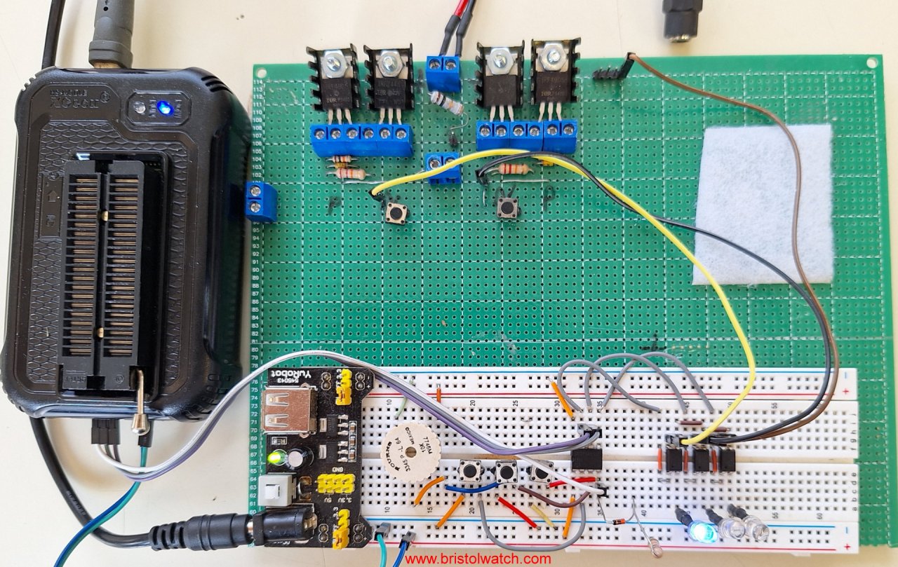
Fig. 1 Microchip PIC12F683 test setup on solderless breadboard.
Click here for larger image.
Introduction PIC12F683 Programming Circuits Tutorial
by Lewis Loflin
Follow @Lewis90068157
On the webpage Pulse Width Modulation Power Control for Microcontrollers explored the use of a PIC12F683 to control power output to a 12-volt LED lamp. Here we look at the PIC12F683 itself and some programming hints.
See Youtube Microchip PIC Projects introductory video.
Welcome and thank you to all the visitors to this page since 2010.
Schematic to the above circuit in Fig. 4 below.
List of images for this project.
The electronics with the high side switch and H-Bridge are the same as the following: Arduino Constant Current H-Bridge Motor Control Use of optocouplers isolates the motor power circuits from the microcontroller allowing the use of multiple controllers.
This webpage is a gateway to PIC programming projects on this website. This section is getting major revisions for 2024. This update is due to changes in the industry.
Four issues are addressed:
1. What PIC programmer does the beginner use? The popular k150 has become useless, as explained here. What replacement programmer does one use? What is ICSP or in-circuit serial programming?
2. What PIC devices does this cover and why? What is a PIC? While centered on the popular PIC12F683, how much money does one spend to get started? What does one need beyond a PIC programmer? See What to buy? at the bottom of page.
3. What programming language to use? This page will focus on PIC assembly with MPLAB IDE v8.92. Also included is the PICBasic Pro (PBP) student edition, which is free but covers only a few devices, one of them the PIC12F683. The programming lessons presented here cover multiple devices due to shared hardware and coding between various PIC controllers.
4. The purpose focus is on hardware control and electronics. These examples center on programming from a hardware and electronics perspective. The focus is on bits, bytes, registers, gates, latches, and multiple combinations: understanding voltages, frequency, and duty cycle. Most importantly, to have fun learning.
What is the definition of a PIC? To quote,
PIC stands for Peripheral Interface Controller or Programmable Intelligent Computer, and it's a registered trademark of Microchip Technology. PICs are a family of microcontrollers that are similar to microprocessors but smaller and more specific in purpose. They're often embedded within devices or consumer products and are much lower power than microprocessors.
PICs are RISC processors which stands for "reduced instruction set computer." The mid-range devices used in these demonstrations have the same 35 instructions., share common register addresses.
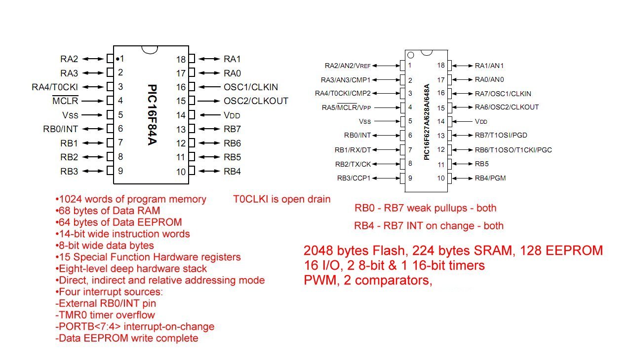
We will learn and program four mid-range devices listed here from least to most complex: PIC16F84A, PIC12F683, PIC16F628A, PIC16F690. The free student version of PIC Basic Pro will program the PIC12F683 and PIC16F630 only. The other devices with pure assembly.
The PIC16F628A can be considered an upgrade to the PIC16F84A. The same is true that the PIC16F690 is an upgrade of the PIC12F683.
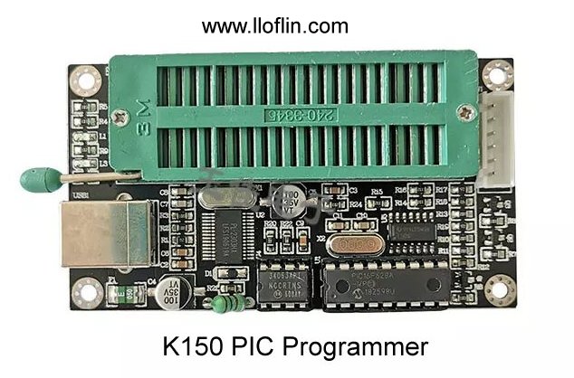
Fig. 2
Beating the K150 Microchip PIC Programmer Fiasco
In 2010, the K150 was the inexpensive way to program the PIC. Those days are gone due to a piracy issue with the Prolific PL2303. These are not original Prolific parts; they shut them down in 2012.
The original drivers below work on Windows XP, Windows 98, 2000, etc., and perhaps Windows 7 32-bit. Windows 10 constantly updates drivers and that is where the problem is. The new drivers disables the legacy hardware. This makes the K150 useless.
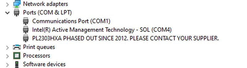
Fig. 2a
To quote:
Nearly every programming cable that is detected by Windows as having a Prolific chip was manufactured with an unauthorized or cloned copy of the Prolific PL2303HXA chip. The latest driver installed by Windows (Vista, 7, 8.1 and 10) is not compatible with these chips. The last compatible Prolific driver was v3.3.2.105 [27/10/2008].
See How to Use K150 PIC Programmer YouTube
See Using the K150 PIC Programmer Windows 10 updated 2024. YouTube
Downloads - there is no warranty use at your own risk:
Driver for K150 PIC programmer: pl1303dtiver.exe
Programming software for K150: K150.rar
Try using the P3200_vista.exe driver first. This was used with Windows Vista. Several users have reported success with this driver. It does work on my Windows 10 Pro.
As an alternative load the driver before using and disconnect the computer from the internet.
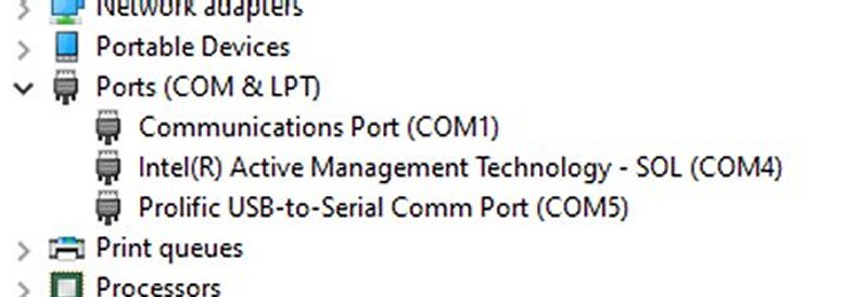
Fig. 2d
Right-click Windows Start, then Device Manager, and one should see the above. Note the Com port number.
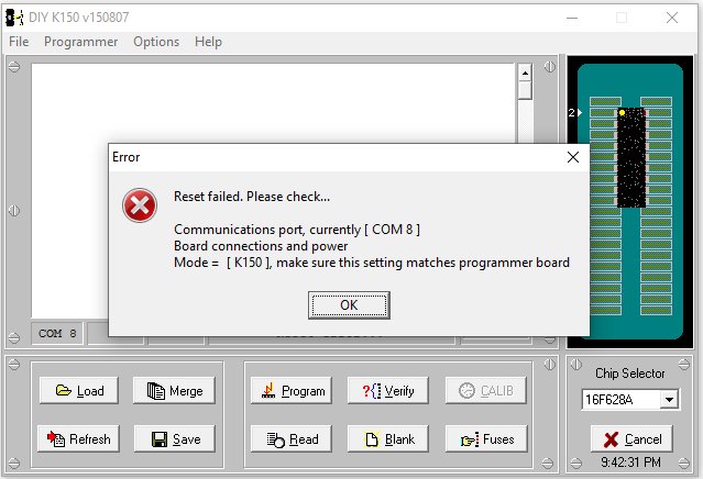
Fig. 2e
Assuming the K150 is plugged in and and the driver is OK, open the K150 software. Most of the time this happens if the port setting is wrong or the driver has been shut off by Prolific.
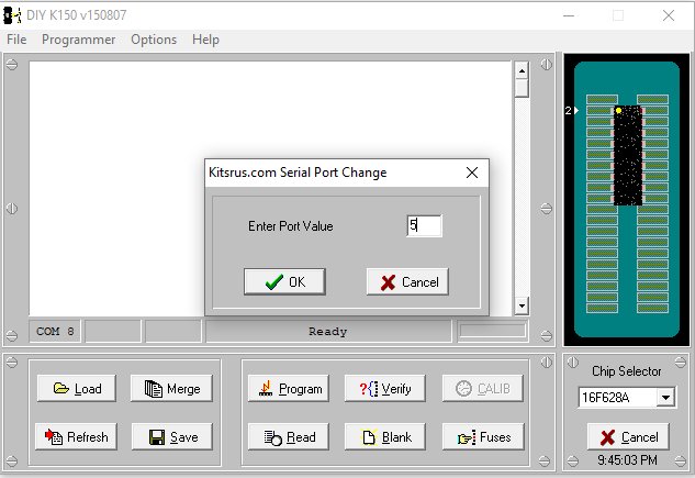
Fig. 2f
To set the correct Com port number select File then Port and the above window will open. Input the correct port number, click OK.
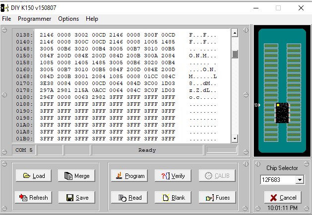
Fig. 2g
A properly functioning K150 PIC programmer is shown in Fig. 2g. A PIC12F683 was inserted in to the ZIF socket as shown and device number was selected. If the wrong device was selected, the device is damaged, etc. an error window will open. In this case the PIC12F683 was read by the K150.
Note the left side of the window near the center 0180. The program was 183 bytes and can be saved as a HEX file. This program operated an LCD display and used 183 out of 2,048 bytes. The 3FFFs are unprogrammed memory cells.
If the code protect has been enabled reading the device produces 0s or 3FFF.
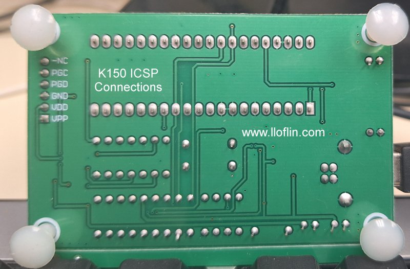
Fig. 2h
In Circuit Serial Programming
The K150 can do in-circuit-serial-programming or ICSP. The connections from the white topside connector are labeled underneath.
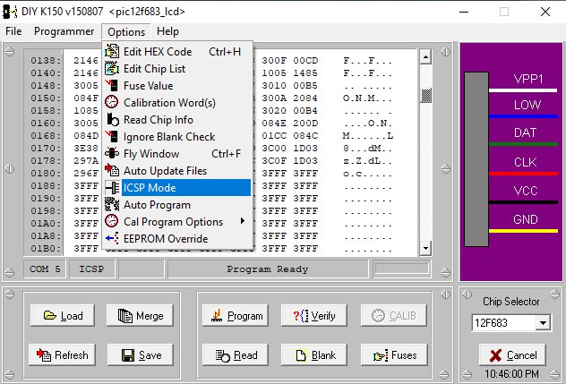
Fig. 2i
To use ICSP select Options ICSP as shown in Fig. 2i.
Add $10-$15 to the cost of a K150 (they are still being sold with pirated PL2303s), get a PICKit2 or PICKit3. See below.
- Operate PIC16F84A TMR0 from RA4/T0CKI Pulse Input
- Toggle ON-OFF LED Based on External Interrupt
- Programming PIC16F84A-PIC16f628a Timers by Example
- Programming PIC16F84A-PIC16F628A TMR0 Interrupts
- Programming PIC16F84A Software Delay Routines by Example
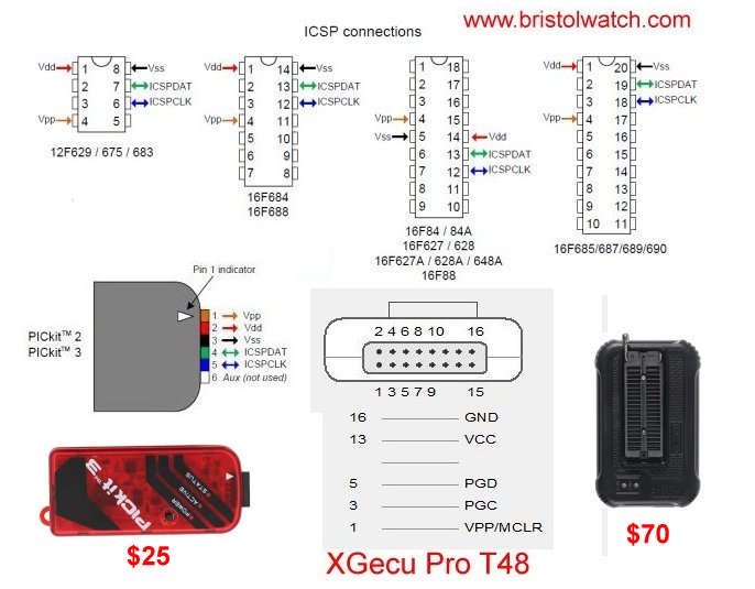
Fig. 3 PIC in circuit serial programming ICSP electrical connections.
The above image illustrates ICSP connections for various PIC controllers and ICSP connections. ICSP stands for "in-circuit serial programming." This technology eliminates having to remove the IC from the solderless breadboard and insert it into a ZIF socket.
Note the original K150 also used ICSP connections. I use the more expensive XGecu T48 that can program almost anything.
Connect as shown, turn off power, program, turn power back on to test.
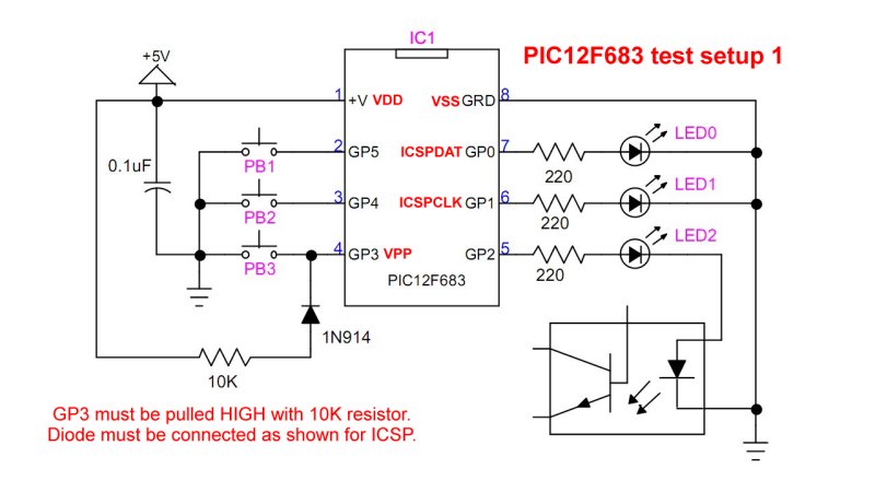
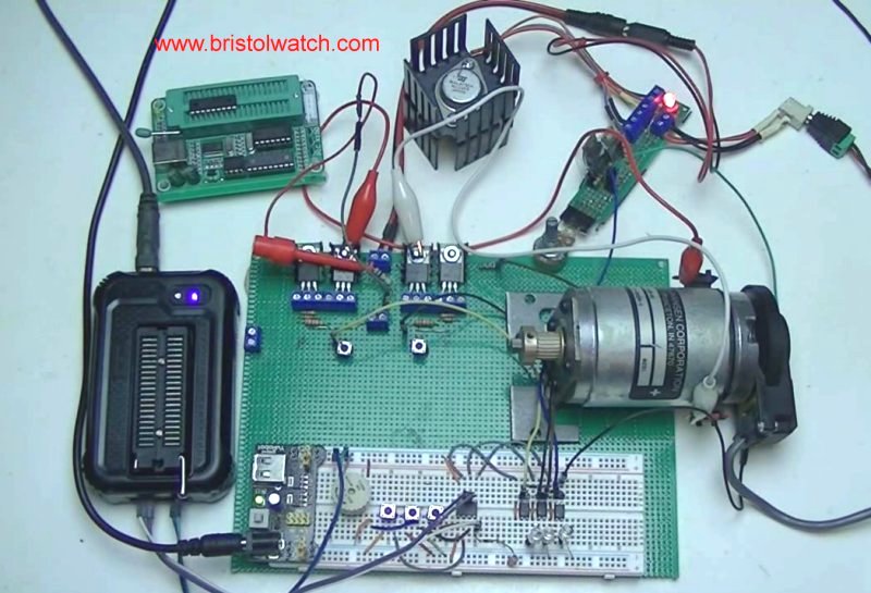
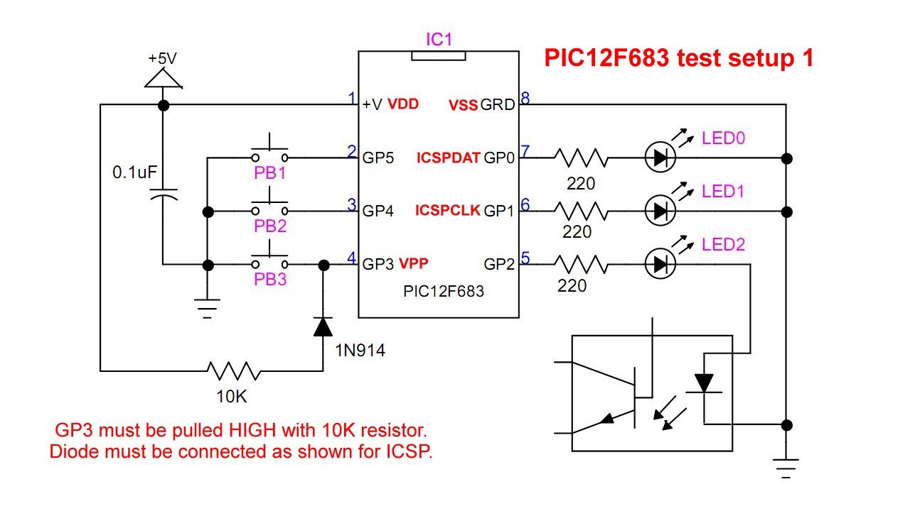
Fig. 4 Mircochip PIC12F683 test setup.
Click here for larger image.
What is needed to get started?
The actual circuit on the prototyping board in Fig. 1. Note the ICSP connections. All three output pins are connected to optocouplers as shown with GP2.
Time to consider what software after a programmer has been chosen. The assembly language will use MPLAB v8.92. It has several features making this an improvement over earlier low end compilers.
To get PIC Basic Pro Student Edition visit https://store.melabs.com/cat/PBP.html. The Student version is free, but limited to the following devices:
PIC12F683
PIC16F688
PIC16F88
PIC16F690
PIC16F886
PIC16F1937
PIC18F2550
PIC18F25K20
PIC18F25K22
An example code for blinking an LED with PIC Basic for the PIC12F683 is as follows:
    LED Con 0   ' Alias GPIO.0 to LED
   ANSEL = 0     ' Set all digital
   CMCON0 = 7    ' Analog comparators off

main:
   high LED      ' Turn on LED connected to GPIO.0
   Pause 500     ' Delay for .5 seconds
   low LED     ' Turn off LED connected to GPIO.0
   Pause 500     ' Delay for .5 seconds
Goto main ' Go back to mainloop

   End
PIC Basic allows direct access to device registers and can be used to help write and debug assembly language code. That is real game changer.
PBP hides most of the underlying code and the above program reveals little. We will go beyond that.
Make lots of notes and comments! The PBP user manual page 23 has an explanation of the I/O pins.
In the PIC12F683 the 6-bit I/O port is labeled GPIO (bank 0, 05h) and the data direction register labeled TRISIO (bank 1, 85h). These labels are predefined by PBP and the MPLAB assembler. MPLAB is used beneath PBP.
Yet in the other devices (PIC1684A, 628A, and 690) label their I/O ports and DDRs as PORTA, PORTB, etc. and TRISA, TRISB, etc. in the same consecutive location address as GPIO and TRISIO of the 683.
One can insert single lines or entire blocks of assembly code into PIC Basic. (Note ";" is a comment.) Example:
; replace single line high LED
@ BSF GPIO, 0 ; 1 byte, 1 uSec. at 4mHz
Multiline assembly code, toggle LED at GPIO bit 0. Uses 2 bytes, 2uSec. at 4mHz.
ASM
    MOVLW 0x01 ; W register = 1
    XORWF GPIO, F ; flip bit state, save in GPIO
ENDASM
The code between "main" becomes the following and does the same thing:
main:

    ASM
        MOVLW 0x01
        XORWF GPIO, F
    ENDASM
    Pause 500     ' Delay for .5 seconds

   Goto main ' Go back to main
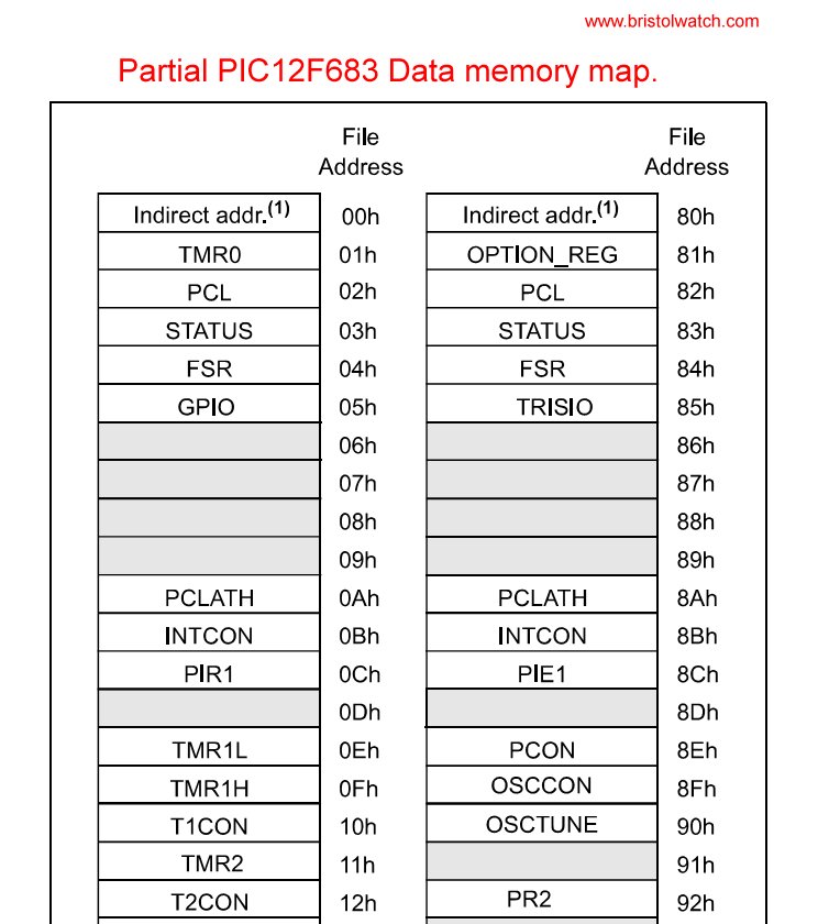
Fig. 5 Partial memory map PIC12F683.
Microchip PICs employ Harvard architecture defined as " a computer architecture with separate storage and signal pathways for instructions and data. It is often contrasted with the von Neumann architecture, where program instructions and data share the same memory and pathways. This architecture is often used in real-time processing or low-power applications.
In simple terms data storage (SRAM above) is separate from program code (flash RAM).
While the registers (files) are 8-bit, the program code uses a 14-bit word labeled 13-0. This is the flash memory where the operating codes are stored.
The following code for PBP blinks the same LED on GPIO 0. This reveals parts of what is hidden from the user. Note the HEX addresses and bank locations in the comments. I also went and defined my circuit with three switches, three LEDs, and turned on the internal pull ups for the switches.
This allows one to test each bit of code one at a time under real program conditions.
    ' DEFINE OSC 4 ; set 4mHz clock PBP
    ' period = 1 / (4mHz. / 4) = 1uSec.

    ' 4MHz Clk, IntOsc, SysClk via IntOsc
    ' exactly same PIC16F690
    OSCCON =  %01100001  ' 8Fh BANK 1

    LED0 var GPIO.0 ' H-bridge side A
    LED1 var GPIO.1 ' H-bridge side B
    LED2 var GPIO.2 ' HIGH = power enable ON

    SW1 var GPIO.5
    SW2 var GPIO.4
    SW3 var GPIO.3

    ' turn on internal pull ups
    OPTION_REG.7 = 1 ' 81h BANK 1
     ' Select pull up pins
    ' 1 = PU ON, 0 = PU OFF
    WPU = %110000 ' 95h Bank 1
    ' external PU on GPIO.3 MCLR

    TRISIO = %111000 ' 85h BANK 1
    ' 1 = input, 0 = output
    ' GPIO.3 always input

    ' BANK 0
    GPIO = 0 ; clear I/O

    ' not in PIC16F84A
    ANSEL = 0  ' 9Fh BANK 1 Set all digital
    CMCON0 = 7 ' 19h BANK 0 Analog comparators off

main:
   ' HIGH LED    ' Turn on LED connected to GPIO.0
    ' flip bit state, save in GPIO.0
    ' 2 uSec. 2 bytes
    ASM
        MOVLW 0x01
        XORWF GPIO, F
    ENDASM

    Pause 500     ' Delay for .5 seconds

   Goto main ' Go back to main

   End
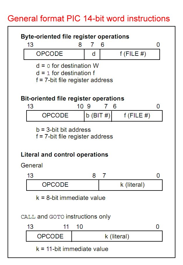
Fig. 6 General format PIC 14-bit word instructions.
First note the PIC12F683 has 2048 bytes of flash and 128 bytes of SRAM. Keep this in mind.
Fig. 6 reveals the word structure stored in the flash memory. This is broken into byte-oriented file operations, bit-oriented file operations, literal and control, and finally CALL and GOTO operations.
Let's begin with CALL and GOTO. These point to a memory address in flash memory. This is literal (k) or 11-bits, or 2^11 = 2,048 the amount of flash RAM in the PIC12F628. But it gets better.
Looking back at this code snippet:
ASM
        MOVLW 0x01
        XORWF GPIO, F
ENDASM
The line MOVLW 0x01 is a literal and control operation, moving 8-bit number 0x01 into the W or working register. The word is divided 8-bit (k) values and a 6-bit opcode.
The line XORWF GPIO, F is a byte- oriented file register operation. This concerns static ram or SRAM.
"GPIO" is predefined label for location 0x05 in bank 0. F is predefined a "1" for file and W is defined a "0". The command will XOR 0x01 in the W register with the value in GPIO register, store the result back in the GPIO register. If W (0) was used instead of F the result would be stored in W.
This would have worked the same as XORWF, 0x05, 1. Note the 14-bit word has 7-bit file address (F #) bits 6-0, a one-bit destination bit (7), and 5-bit OPCODE. Take 2^7 = 128 or 0-127 bank0 and 0-127 bank 1. Notice the SRAM in bank 0 ends at 0x7F or 127.
Because of the 7-bit word limitation, the SRAM is "banked" with the bank selected by bit 5 (RP0) in the STATUS register, at 0x03, in bank 0, and 0x83 in bank 1. STATUS in both banks is the same thing.
STATUS is a label and all labels are case sensitive - sTATUS will return an error. This bank issue is taken care of by PBP in the background. Note the following code examples in assembly. Commands such as MOVWF, etc. are not case sensitive.
; switch to bank 0
    BCF STATUS, 5 ; bit 5 = 0 in STATUS register.
    banksel 0 ; same as above

; switch to bank 1
    BSF STATUS, 5 ; bit 5 = 1 in STATUS.
    banksel 1 ; same as above

; use define to save time
    #define BANK0 BCF STATUS, 5
    #define BANK1 BSF STATUS, 5

; going to Bank 1 now is simply,
    BANK1

; example GPIO.0 - GPIO.5 is not defined in assembly
; do it yourself

#define GPIO.0 GPIO, 0
    BSF GPIO.0 ; LED on.

; even better
    #define ON bsf GPIO,
    #define OFF bcf GPIO,

    ON LED
The snippet BSF STATUS, 5 is an example of a bit oriented register instruction. This has a 7-bit SRAM address (0-127), 3-bit device bit address (0-7), and 4-bit opcode.
Below is the code in assembly for blinking our LED. I added in my delay routines as subroutines. The program used 50 bytes out of 2048 on the PIC12F683.
;==============================
	list P=12F683, ST=OFF   ; Turnoff Symbol Table in List file.

	errorlevel  -302  ; Ignore error message Bank 1.
;==============================

        #include   <p12f683.inc>

        ; this must be a single line or compiler error
   __config _INTOSCIO & _WDT_OFF & _PWRTE_ON & _MCLRE_OFF & _CP_OFF & _CPD_OFF & _BOD_NSLEEP & _IESO_OFF & _FCMEN_OFF

	LED0 EQU 0
	LED1 EQU 1
	LED2 EQU 2
	PB0 EQU 5
	PB1 EQU 4
	PB2 EQU 3

	; Assign each SRAM register from Bank 0.
	CBLOCK  0x20
	temp1
	CNT1
	CNT2
	CNT3
	CNT4
	ENDC ; Conclude Bank 0 RAM assignments.

	; for compiler, doesn't use memory
	#define BANK0 banksel 0
	#define BANK1 banksel 1

	#define ON bsf GPIO,
	#define OFF bcf GPIO,

	ORG     0x000  ; processor reset vector
	goto    setup  ; go to beginning of program

	ORG     0x004   ; interrupt vector location
	retfie            ; return from interrupt

setup

	BANK1    ; Switch to Bank 1.
	MOVLW   B'01100001' ; 4MHz Clk, IntOsc, SysClk via IntOsc
	MOVWF   OSCCON
	CLRF    ANSEL ; Set all I/O pins to Digital.
	; GPIO 6-bit port GPIO.0 - GPIO.5
	; GPIO.0 - GPIO.2 output; GPIO.3 - GPIO.5 input
	; 1 = INPUT, 0 = OUTPUT
	MOVLW B'111000'
	MOVWF TRISIO ;
	; pull ups
	BCF OPTION_REG, 7 ; turn on PU
	MOVLW B'111000' ; 1 = PU on.
	MOVWF WPU
	BANK0
	MOVLW   b'00000111' ; Turn off Comparator.
	MOVWF   CMCON0
	CLRF    GPIO

main

	ON LED0
	movlw d'5'  ; same as using .5 for decimal
	call Wx100ms ; W * 100mS

	OFF LED0
	movlw d'5'  ; same as using .5 for decimal
	call Wx100ms ; W * 100mS

goto main

;**************************	;Delay routine.
; Calculating a 1mSec delay. 4mHz is divided by 4 internally to
; At 4mHz / 4 = 1uSec. 1000 uSec. = 1 mSec.
; GOTO uses 2 cycles DECFSZ 1 cycle = 3 cycles or 3uSec.
; 3 * 82 * 4 =~ 1000uSec. or 1mSec.

DELAY_1ms
	; 4 mHz crystal
	MOVLW .4
	MOVWF CNT1
	MOVLW .82
	MOVWF CNT2
	DECFSZ CNT2, F
	GOTO $-1 ; count 82 times at ~3.05 uSEC per count
	DECFSZ CNT1, F
	GOTO $-5
	RETURN

DELAY_100ms
	MOVLW .100 ; value * DELAY_1ms = total delay
	GOTO $+2
Wx1ms ; W* 1mS
	MOVWF CNT3 ; 1mS * W
	CALL DELAY_1ms
	DECFSZ CNT3, F
	GOTO $-2
	RETURN

DELAY_1sec
	MOVLW .10 ; value * DELAY_1ms = total delay
	GOTO $+2
Wx100ms ; W * 100mS
	MOVWF CNT4 ; 100mS * W
	CALL DELAY_100ms
	DECFSZ CNT4, F
	GOTO $-2
	RETURN

end
To see the entire program shown in the video see analog.asm for more sample code.
YouTube video: My Home Built PIC16F628A Dev. Board
For a video demo of this page see PIC12F683 Microcontroller Circuits on YouTube.
To see the entire program shown in the video see analog2.asm updated 2024.
DEC to HEX https://www.rapidtables.com/convert/number/decimal-to-hex.html
- Programming PIC16F84A-PIC16F628A Interrupts by Example
- PIC16F84A-PIC16F628A Pull Up Resistors with Interrupts
- Programming PIC16F84A-PIC16f628a Timers by Example
- Programming PIC16F84A-PIC16F628A TMR0 Interrupts
- Programming PIC16F84A Software Delay Routines by Example
- Microchip PIC related videos:
- How to Use K150 PIC Programmer
- Microchip PIC16F628A Basic H-Bridge Motor Control
- Microchip PIC16F628A Counts BCD on 8 LEDs
- PIC16F84A Operates H-Bridge Motor Control
- PIC16F84A Operates MOSFET H-Bridge
- Using Velleman K8048 PIC Development Board
- Arduino Port Registers Revisited
- Digispark ATtiny85 with MCP23016 GPIO Expander
- Safely Build Program a H-Bridge
- Build H-Bridge Motor Control Without Fireworks
- MOSFET H-Bridge for Arduino 2
- Microchip PIC16F84A H-Bridge Motor Control
- Microchip PIC16F628A Basic H-Bridge Motor Control
- PICAXE Operates H-Bridge Motor Controller
- PICAXE Microcontroller Controls Motor Speed - Direction
- PICAXE Projects
What to by?
What PIC chip does one use? While the PIC12F683 is referenced here, all five devices I use have interchangeable code. The difference is built in hardware "modules". The more complex the part, the more internal modules or circuitry.
PIC16F57-I/SP 20 IO pins, up to 20mHz. clock, 28 pin DIP. At Digikey, $1.38 ea. 2K flash memory, 72 bytes SRAM, single timer, 20 I/O pins, 28-pin dip. See image PIC16F57_pins.jpg. Has no internal pull ups or interrupts.
While very simple to learn, this will be assembly only.
PIC16F84A-04I/P has 13 IO pins. up to 20mHz. 18 pin DIP. Digikey, Mouser $5.46 ea. - yikes! $2 Ebay. 1K flash, 64 bytes SRAM, pull ups, interrupts, same timer.
Both of the above require a separate crystal plus 2, 22pF capacitors. Those below can use external crystals but have internal oscillators up to 8mHz. For example the PIC16F628A:
Internal and external oscillator options: - Precision internal 4MHz oscillator factory calibrated to ±1% - Low-power internal 48kHz oscillator - External Oscillator support for crystals and resonators.
PIC16F628A Digikey $2.74, Mouser $3.07, and $2 ea. Ebay. For pin connections and specs see image pic16f84a_pic16f628a.jpg. The PIC6F628A is a major upgrade to the PIC16F84A and more complex. For the novice is harder to learn.
PIC12F683-I/P Mouser $2, Ebay $2. Internal oscillator factory calibrated to ±1%, typical - Software selectable frequency range of 8MHz to 125kHz - Software tunable.
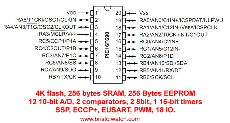
PIC16F690-I/P Digikey $2.76, Ebay $2 ea. This has so many features, see the following image PIC16F690.jpg
I checked the versions of PICs used here and they are still manufactured. I bought all of my devices from Ebay and had no problems.
How about building basic PIC circuits? All devices must be "DIP" packages to fit a solderless breadboard. One will various parts, and some test equipment if starting from nothing.
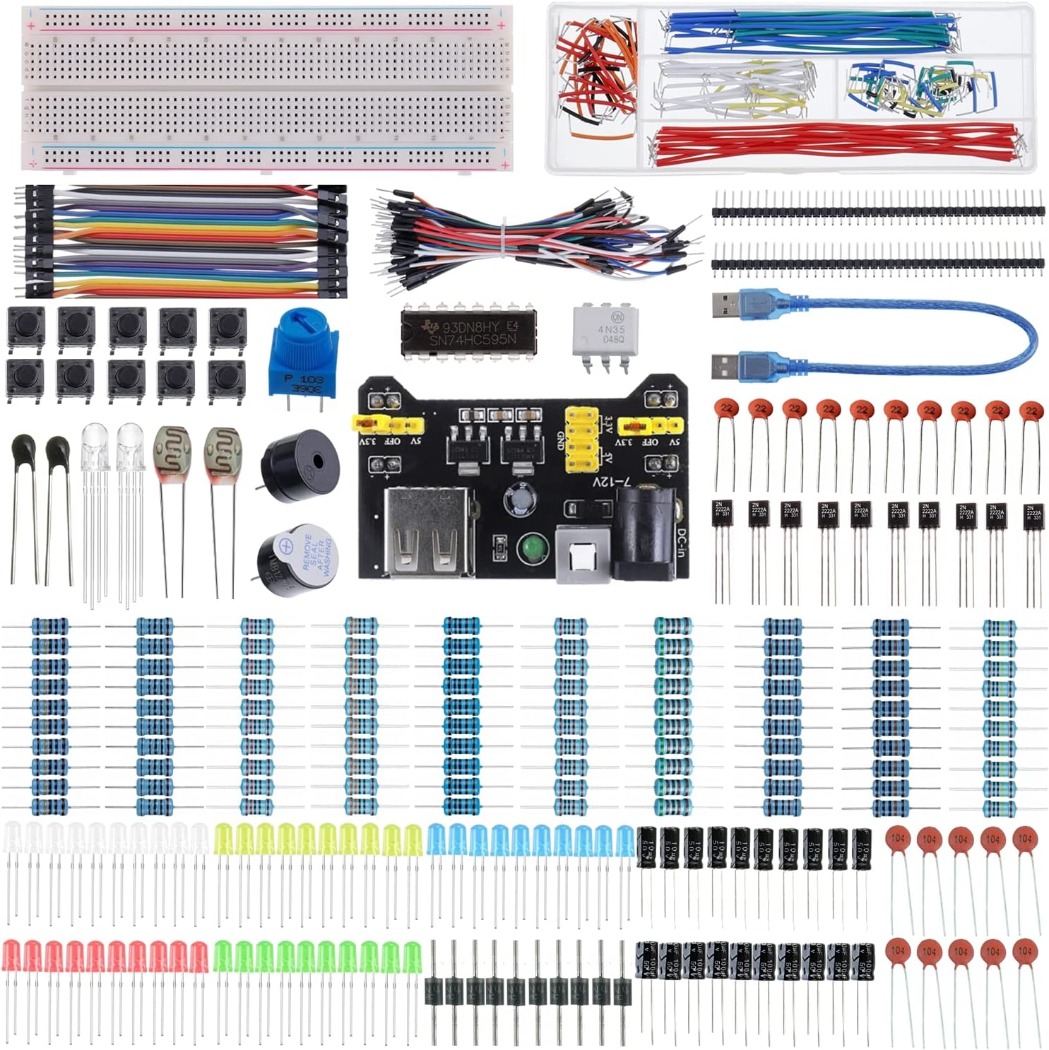
Amazon search "electronic parts assortment." One assortment from BOJACK for $16 (Amazon Prime) has all needed parts including solderless breadboard, power supply module, about 480 parts of all types. This is a sample as of 8/2/2024. See the image parts_assortment.jpg. Link www.amazon.com. There are others selling the same thing.
The power supply module is shown on the left side of my test circuit. It can use a 5-volt cell phone charger supply via the USB connector. Or Amazon search "DC 9V Power Supply 2.1mm x 5.5mm barrel connector."
Optional: Neoteck 2000 Counts Digital Multimeter Voltmeter Tester with NCV, LCD for AC/DC Voltage & Current, Resistance, Capacitance, Frequency, Temperature, Duty Cycle, Continuity, Diode, etc.. Amazon ~$26. The frequency counter and duty cycle functions are very useful.
Optional: A good basic logic probe is also very useful. I use an Elenco LP-560. ($25 Amazon)
PIC16F57 projects.
- PIC16F57 LCD Counter – Real Hardware Binary and Decimal Display
- PIC16F57 using TMR0 with External 60Hz or 120Hz Clock
- 8-Bit LCD Interface with PIC16F57: Binary and Decimal Counter in C (XC8)
- PIC16F57 Serial LCD and 4x4 Keypad Demo
- Simulate PLC Ladder Logic with PIC16F57 Microcontroller – Simple C Example
The next three pages focuses on Timer0 and interrupts in the PIC16F84A
- PIC16F84A – TMR0 with External 60Hz Timebase on RA4 (Pin 3)
- PIC16F84A Interrupt Examples – RB0 and RB4–RB6 with LED Toggling
- Comparing PORTB Pull-Ups and Interrupts: PIC16F84A vs. PIC16F628A
- Using Timer1 on the PIC16F628A as a Pulse and Frequency Counter
- PIC16F628A Interrupt-on-Change Debounced Button Input on RB4
- PIC16F628A – Interrupt-Driven 1Hz Square Wave from 60Hz Input
- Using a 32.768 kHz Crystal with Timer1 on the PIC16F628A
- Interfacing HD44780 LCD with PIC16F628A in 4-Bit Mode
- PIC16F628A: Displaying Decimal Numbers on LCD 4-Bit Mode
- PIC16F628A PWM Output with Fade Example – 1 kHz LED Control
Web site Copyright Lewis Loflin, All rights reserved.
If using this material on another site, please provide a link back to my site.