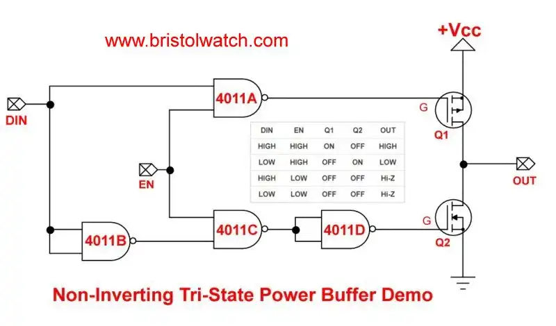
Fig. 1 Tri-state buffer schematic.
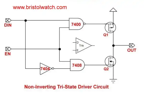
Non-Inverting Tri-State Buffer-Switch Demo Circuit
by Lewis Loflin
This page demonstrates using a single integrated circuit with 2 MOSFET output transistors.
To better understand the operations of this circuit as far as MOSFET output see High Current Tri-State MOSFET Driver Circuit. This was not a tri-state circuit with the output either HIGH-LOW.
This has three output levels: HIGH (Vcc), LOW (GND), and Hi-Z.
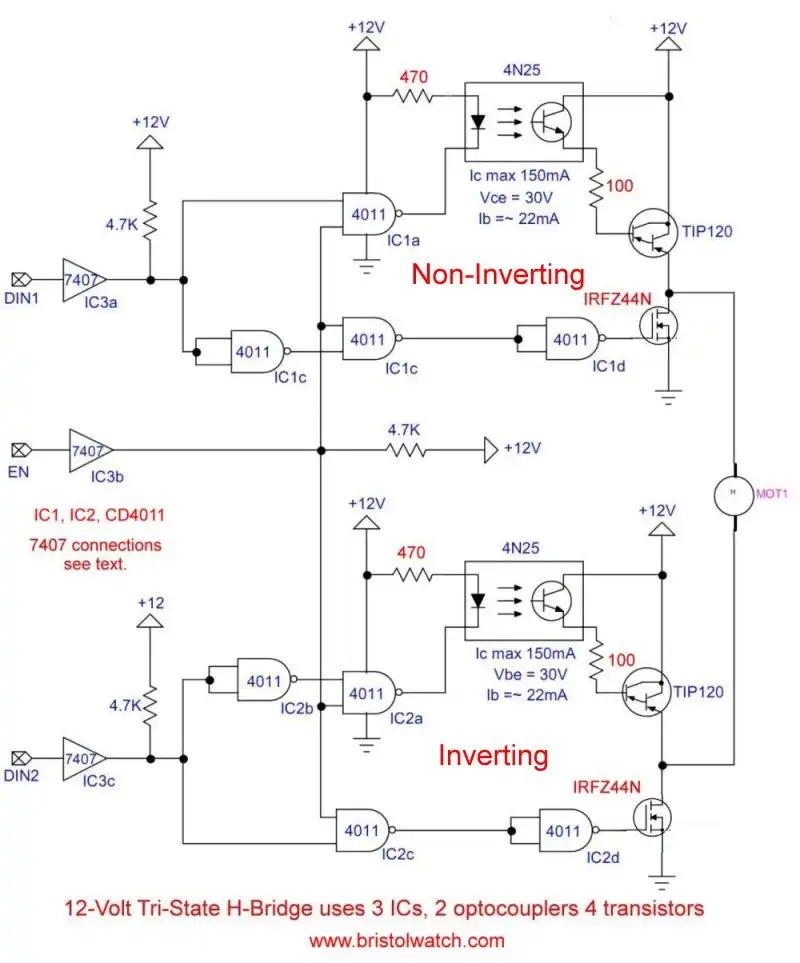
The ultimate goal is the H-Bridge shown as hb_big2.jpg
Also, the original tri-state circuit required three separate integrated circuits. This uses a single integrated circuit to do the same thing.
Fig. 1 illustrates using a single CD4011 integrated circuit with quad (4), 2-input NAND gates. A CD4011 operates from 3-15 volts.
CD4011B and CD4011D operate is inverters - HIGH in = LOW out and vice-versa.
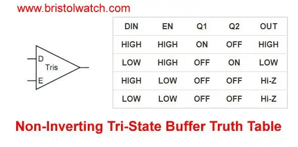
Fig. 2 Tri-state MOSFET output buffer truth table.
Fig. 2 is the truth table for the circuit in Fig. 1. What is not shown in Fig. 1 is the voltage connections for the CD4011 and +Vcc.
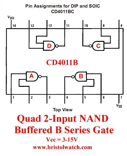
Fig. 3 CD4011 Pin Connections
If this circuit is connected to 5-volts then direct connection to a microcontroller such as PICAXE, Arduino, and PIC are simple direct connections.
When the gate to Q1 LOW, Q1 will turn on. When the gate of Q2 is HIGH, Q2 will turn on.
Both Q1 and Q2 must never be turned on at the same time!
If we use a 12-volt motor, etc. then the CD4011 voltage must also be 12-volts. The problem is direct connection to a 5-volt microcontroller won't work.
That requires a separate interface circuit. Q2 can remain as it is, it's the Q1 circuit that is the problem. I'll assume a 5-volt supply for the digital circuits.
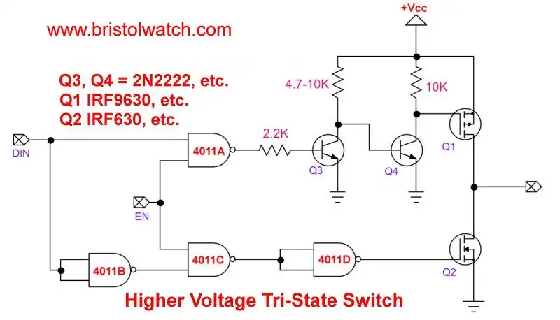
Fig. 4 Tri-State switch with NPN transistors for higher voltage output.
Fig. 3 illustrates the use of 2 NPN bipolar transistors and 3 resistors for higher voltage output. Remember +Vcc is NOT the 5-volt supply for the digital circuit. This is the output voltage that can't exceed Vgs of the P-channel MOSFET.
The truth is identical to Fig. 2.
For more on power MOSFET switches see the following:
- Exploring Solid State Relays and Control Circuits
- Comparing Photo Triac, Photo SCR Opto-Couplers
- Light Activated SCR Based Optocouplers Circuit Examples
- Silicon Controlled Rectifier Review and Circuits
- Silicon Controlled Rectifiers Connected as Power Triacs
- Insulated Gate Bipolar Transistor IGBT Circuits
- Current Limiter Circuits for Opto-Coupler LEDs
- VOM1271 Photovoltaic MOSFET Driver Circuits
- Current Limiter Allows Safe Testing of Zener Diodes, LEDs
- 3 Amp LM741 Op-Amp Constant Current Source
- Bidirectional Solid State Relay Circuits
- Simple Solid State Relay for Low Power LED 120V Lamps
- Build High Power MOSFET Directional Switch Relay
- Optical Isolation of H-Bridge Motor Controls
- All NPN Transistor H-Bridge Motor Control
- Basic Transistor Driver Circuits for Micro-Controllers
- ULN2003A Darlington Transistor Array with Circuit Examples
- Tutorial Using TIP120 and TIP125 Power Darlington Transistors
- Driving 2N3055-MJ2955 Power Transistors with Darlington Transistors
- Understanding Bipolar Transistor Switches
- N-Channel Power MOSFET Switching Tutorial
- P-Channel Power MOSFET Switch Tutorial
- Build a Transistor H-Bridge Motor Control
- H-Bridge Motor Control with Power MOSFETS
- More Power MOSFET H-Bridge Circuit Examples
- Build a High Power Transistor H-Bridge Motor Control
- H-Bridge Motor Control with Power MOSFETS Updated
- Opto-Isolated Transistor Drivers for Micro-Controllers
- Comparator Theory Circuits Tutorial
- Constant Current Circuits with the LM334
- LM334 CCS Circuits with Thermistors, Photocells
- LM317 Constant Current Source Circuits
- TA8050P H-Bridge Motor Control
- All NPN Transistor H-Bridge Motor Control
- Basic Triacs and SCRs
- Comparator Hysteresis and Schmitt Triggers
- Comparator Theory Circuits Tutorial
- Photodiode Circuits Operation and Uses
- Optocoupler MOSFET DC Relays Using Photovoltaic drivers
- Connecting Crydom MOSFET Solid State Relays
- Photodiode Op-Amp Circuits Tutorial
- Optocoupler Input Circuits for PLC
- H11L1, 6N137A, FED8183, TLP2662 Digital Output Optocouplers
- Optical Isolation of H-Bridge Motor Controls
- All NPN Transistor H-Bridge Motor Control
© Copyright 2019 Lewis Loflin E-Mail