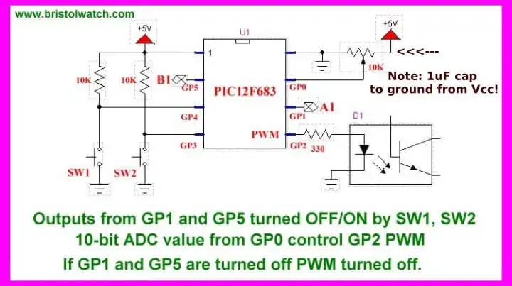
Fig. 1 Mircochip PIC PIC12F683 test setup.
Introduction PIC12F683 Programming Circuits Tutorial
In Pulse Width Modulation Power Control for Microcontrollers we explored the use of a PIC12F683 to control power output to a 12-volt LED lamp. Here we look at the PIC12F683 itself and some programming hints.
YouTube video: My Home Built PIC Dev. Board
For a video demo of this page see PIC12F683 Microcontroller and Circuits on YouTube.
This test circuit (Fig. 1) employs a Mircochip PIC PIC12F683 using its analog-to-digital converter (ADC) taking the analog value of a potentiometer converting the 0-5V reading into a 10-bit value from 0-1023. That 10-bit value is sent to pulse-width-modulation module at pin GP2.
That value sets the duty cycle (on time vs. period) of a 250Hz square wave generated by an internal timer. Period = 1/F = 1/250 = 4mSec.
K150 PIC Programmer
- Microchip PIC related:
- How to Use K150 PIC Programmer
- Microchip PIC16F628A Basic H-Bridge Motor Control
- Microchip PIC16F628A Counts BCD on 8 LEDs
- PIC16F84A Operates H-Bridge Motor Control
- PIC16F84A Operates MOSFET H-Bridge
- Using Velleman K8048 PIC Development Board
Downloads - there is no warranty use at your own risk:
Driver for K150 PIC programmer: pl1303dtiver.exe
Programming software for K150: K150.rar
I have included a pre-made template with the basic setup and configuration already done with a couple of delay routines pre-written. (We will go over those.) I'll be programming in assembly for a number of reasons in particular cost and flexibility. Also because what few assembly examples available are just terrible.
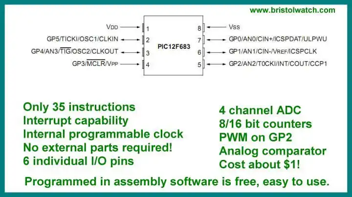
Fig. 2 Features and pin connections of the PIC12F683.
Fig. 2 shows just some of the features of the PIC12F683 which includes 6 programmable I/O pins, 4-channel analog-to-digital converters, and 1 each PWM and comparator modules. It has far more features than a PIC16F84A and has ADCs the PIC16F628 lacks. It has 2048 bytes of flash ram more than enough for most applications.
As a bonus its programmable internal "clock" requires no external parts just a 3-5 volt power supply. (See Fig. 1) I designed this with a 4mHz clock (default then internally divided by 4) which provides a clock cycle time of 1uSec - the 35 instructions are mostly 1 cycle except branches such as GOTO.
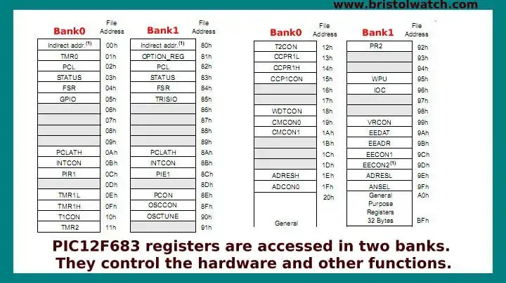
Fig. 3 Register banks of the PIC12F683.
New October 2016:
- Programming PIC16F84A-PIC16F628A Interrupts by Example
- PIC16F84A-PIC16F628A Pull Up Resistors with Interrupts
- Programming PIC16F84A-PIC16f628a Timers by Example
- Programming PIC16F84A-PIC16F628A TMR0 Interrupts
- Programming PIC16F84A Software Delay Routines by Example
- Microchip PIC16F84A H-Bridge Motor Control
- Microchip PIC16F628A Basic H-Bridge Motor Control
- PICAXE Operates H-Bridge Motor Controller
- PICAXE Micorcontroller Controls Motor Speed - Direction
- PICAXE Projects
- Arduino Port Registers Revisited
- Digispark ATtiny85 with MCP23016 GPIO Expander
- Safely Build Program a H-Bridge
- Build H-Bridge Motor Control Without Fireworks
- MOSFET H-Bridge for Arduino 2
PIC12F683 registers are accessed in two banks. They control the hardware and other functions. The I/O pins are labeled GP0 - GP5. they can be programmed as shown in fig. 2 by setting and clearing bits in the associated register. The p12f683.inc file defines names based on the register/bank labels. Look at this code that will setup the internal clock in the template. Note that I'm using MPLAB v8.92 compiler which changes labels and code one types into machine code (a HEX file) programmed into the PIC.
BANKSEL OSCCON          ; Switch to Bank 1.
MOVLW   b'01100001'     ; 4MHz Clk, IntOsc, SysClk via IntOsc
MOVWF   OSCCON
Note 1: anything after ";" is a comment and ignored. Use lots of comments to make notes to yourself!
Note 2: commands such MOVLW, MOVWF, and BANKSEL are NOT case sensitive. One could use say "movlw" or "MOVlw", etc. Be consistent!
Note 3: the PIC series uses mainly 8-bit registers that can hold a number form 0-255 decimal. The compiler doesn't care what number base one uses so 255 can be d'255' or .255 for decimal; b'11111111' or 0b11111111 for binary, or 0xff or 0xFF for hexadecimal. I don't know about OCTAL - the compiler doesn't seem to care when I tried 0777.
Note 4: the include file in the template defines names to a number. Look at the bank table in figure 3 and notice "OSCON" (or oscillator control register) is in Bank 1 location Ox8F. Otherwise one would have to define the label themselves (OSCON EQU 0x8F) or simply use "MOVWF 0x8F".
Note 5: defined names from the include file ARE case sensitive! So using "oscon" etc. will cause a compiler error.
Note 6: one must be in the correct bank to change register data, bits, etc. The STATUS register (0x03 and 0x83) is shared by BOTH Bank0 and Bank1 respectively. Bit 5 (labeled RP0) is the bank select bit. Clearing the bit (0) puts one in bank 0 and setting the bit (1) puts one in bank 1:
BSF STATUS, RP0 ; selects bank 1 by setting bit 5 - Rp0 is defined as 5
; or
BCF STATUS, RP0 ; select bank 0
BSF is "bit-set file" while BCF is "bit clear file". For more on the STATUS register see P11 in the data sheet - make sure you have that data sheet!
So to change data in the OSCON register (P19 in data sheet) I must be in bank 1. BANKSEL saves a lot of trouble because the compiler knows what's in what bank and does the work for you. So if I needed to change a bit, etc. in say TMRO (bank 0 0x01) use "BANKSEL TMRO" and forget this RP0 business.
Note 7: the W or working register. Think of the W register as a box that can hold any combination of 8 zeros and ones. I load a number from 0-255 into the box and deliver it to the correct register (ex. OSCON) and deposit it there. Most instructions the programmer must specify if the result is to be stored in the W register or a file: Ex. DECFSZ filename, 0 (or W) stores the result in W; DECFSZ filename, 1 (or F) stores the result in the file register.
So what did my three lines of code in 3uSec. do? I selected bank 0, moved a literal number in binary into the W register, then the PIC W register moved that byte to the OSCON register from the W register.
Now I'm sure some are quaking in their boots - I have to do all this stuff??? That's why I'm here to help others avoid the nightmares I went through when I taught myself PIC assembly. The basic compilers are EXPENSIVE and the MPLAB C compiler has some copyright and licensing issues. It makes no sense to use anything other than assembly for these small controllers - larger ones yes.
Once one learns assembly on one PIC it works on the others. See my section PIC16F628A in Assembly.
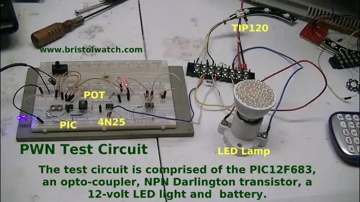
Fig. 4 Test setup using a Microchip 12F683 to demonstrate pulse width modulation.
Programming the PIC12F683 and Others
Hardware operation and pulse-width modulation is covered in Pulse Width Modulation Power Control for Micro-controllers. As shown in figure 1 switches are connected to GP3 and GP4 programmed as digital inputs. The pins are pulled to +5V (HIGH) through two 10K resistors. When a switch is pressed the inputs go to 0V (LOW).
An opto-coupler is connected to GP2 programmed as an pulse-width modulation output. Output is "toggled" ON/OFF whenever SW1 and/or SW2 is pressed. GP1 and GP5 are also "toggled" ON/OFF respectively. That was used to control a H-bridge motor control. The opto-coupler isolates the 12-volt circuit from the 5-volt PIC.
A potentiometer is connected to GP0 programmed as an analog input using the 10-bit ADC module. This 10-bit value is read and used to set the duty cycle for the 10-bit PWM module at GP2.
Think of the PIC12F683 or any other PIC as a collection of programmable electronic modules along with the micro-controller. PIC like the ATMEGA168, etc used by Arduino are known as RISC processors - reduced instruction set computer. There are only 35 instructions in this case.
Let's dive deeper into programming. Refer to template.asm and study the specification sheet.
CBLOCK  0x20 ; Assign each reg. from Bank 0 RAM area.
count1
count2
count3
count4
temp
RESULTHI
RESULTLO
ENDC        ; Conclude Bank 0 RAM assignments.
Referring to figure 3 I'm using static ram locations starting at 0x20 for variables. I always declare several in case I need them. The function "CBLOCK" saves one from declaring each variable individually using EQU or using the hexadecimal number itself.
ORG     0x000     ; processor reset vector
GOTO    setup     ; go to beginning of program

ORG     0x004     ; interrupt vector location
; isr code can go here or be located as a call subroutine elsewhere
RETRIE           ; return from interrupt
When the controller resets the address counter starts at 0x000. The label "setup" points to a flash ram location for the setup routine defining mainly hardware functions. That location is done by the compiler.
ORG 0x004 is the interrupt vector pointing to what is known as an ISR or interrupt service routine. The PIC12F683 has a number of programmable hardware interrupts. Once an interrupt occurs the PIC stops what it's doing, saves the present location-count address on the STACK, then services the ISR.
One can call another subroutine or perform the function here. One must have RETIE that pulls the original address from the STACK and allows PIC to return to what it was doing.
setup

BANKSEL OSCCON          ; Switch to Bank 1.
MOVLW   b'01100001'     ; 4MHz Clk, IntOsc, SysClk via IntOsc
MOVWF   OSCCON

BANKSEL CMCON0          ; Switch to Bank 0.
MOVLW   b'00000111'     ; Turn off Comparator.
MOVWF   CMCON0

BANKSEL ANSEL           ; Switch to Bank 1.
CLRF    ANSEL           ; Set I/O pins to Digital.

; Define inputs & outputs.
CLRF   TRISIO ; all output
BSF	   TRISIO, GP3 ; GP3 input
BSF	   TRISIO, GP4

BANKSEL GPIO    ; Switch to Bank 0.
CLRF    GPIO

; This code block configures the ADC for polling,
; Vdd reference, Frc clock and GP0 input.

BANKSEL TRISIO;
BSF     TRISIO, 0 ; Set GP0 for ADC input
; ANSEL ; 0x9F P32
MOVLW   0b01110001 ; ADC Frc clock,
IORWF   ANSEL ; and GP0 as analog
BANKSEL ADCON0 ; 0x1F
MOVLW   0b00000001 ; Left justify,
MOVWF   ADCON0 ; Vdd Vref, An0, On
CALL    delay_1ms ; Acquisition delay

; setup PWM
; CCP1CON in bank 0 bits 4-5 are LSB of 10-bit PWM

MOVLW	b'00000111'
MOVWF	T2CON ; turn on TMR2 prescale 16 - frequency
MOVLW	d'127' ; duty cycle = TMR2 = CCPR1L:CCP1CON 5:4
MOVWF	CCPR1L
MOVLW	b'00001100'
MOVWF	CCP1CON 	; turn on PWM

GOTO loop ; jump to main program "loop"
The above does the same thing as setup() does in Arduino and is done only once unless called. I defined the 4mHz "clock", turned off the comparator module, set all the I/O to digital. With TRISIO in bank 1 I defined GP3 and GP4 (set the corresponding bits) as inputs all other pins as outputs. I clear registers such as GPIO (bank 0) and ANSEL (analog select bank 1) to make sure they are in a known state. Failing to do that can create all kinds of problems.
Note: GP3 can only be programmed as an input!
Then I setup GP0 as an ADC input, then the PWM module is setup for 250Hz through timer 2 (T2CON) while the 10-bit value to control the duty cycle is in registers CCPR1L and CCP1CON in bank 0.
Setup is the hardest thing to do so start with my general template and learn to do one thing then go onto another.
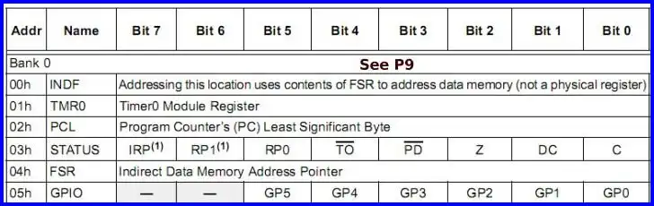
Fig. 5 Part of Bank 0 Microchip 12F683.
loop
; do something
GOTO loop
The above is the very same thing the Arduino loop does in C. Let's try something simple like blink a LED connected to pin GP1 connected through a resistor to ground. To make the program go we need to store a HIGH in the GPIO register at GP1 or bit 1. We wait for while, then store a 0 in bit 1 or GP1 and wait again. At the end of the sequence "GOTO loop" brings us back to the beginning. Note the register configuration for part of bank 0.
We should be in bank 0 and if not sure use "BANKSEL GPIO". When we use commands like BSF and BCF we go DIRECTLY to the register in this case GPIO or 0x05. Note figure 5.
loop

BSF GPIO, GP1 ; same as BSF 0x05, 1 - bit 1 HIGH LED on.
; wait
BCF GPIO, GP1 ; same as BCF 0x05, 1 - bit 1 LOW LED off
; wait

GOTO loop
As written the ON-OFF time is 2uSec. and can only be seen on an oscilloscope. Now we come to the use of subroutines. Build a collection of small debugged routines and use them to build other larger routines through the use of CALL. We need a delay routine to slow the process down so we can see something. Back in setup there was a CALL to delay_1ms.
; Calculating a 1mSec delay. 4mHz is divided by 4 internally to
; 1,000,000. Take reciprocal divide 1mSec by 1uSec = 1000.
; GOTO uses 2 cycles, DECFSZ 1 cycle.

delay_1ms
	; 4 mHz crystal
	movlw D'2'
	movwf count1
aa	movlw D'167'
	decfsz count2, F ; inner loop
	goto $-1 ; two cycles
	decfsz count1, F ;
	goto aa
	return
What we have is a subroutine delay_1ms using what is called a software loop. We have two loops one with count1 = 2 and the other count2 = 167. (Both in decimal.) These are the static RAM locations we declared earlier with CBOCK 0x20.
What DECFSZ does is decrement the count1 or count2 and check the Z flag in the STATUS_REG register (0x03) bit 2 and if set (1) means the result of the last decrement is zero and will skip the following instruction goto $-1 and exit the loop.
With DECFSZ count, F - F means store the result in the "count" register while a W will store the result in the internal working register W. Many of instructions do this.
Each DECFSZ and GOTO takes 3uSec. 167 times for about 500uSec. total. The outer loop (count = 2) goes through the 500uSec loop twice for a delay of about 1mSec - thus the name delay_1ms. (Use names that make sense.)
delay_250ms
	movlw d'250'
	movwf count1
aa	call delay_1ms
	decfsz count1, F
	goto aa ; aa can be left out use "goto $-2"
	return
Now we used a 2nd delay routine that calls delay_1ms 250 times. So now we complete our program where the LED will blink ON-OFF every half-second.
loop

BSF GPIO, GP1 ; same as BSF 0x05, 1 - bit 1 HIGH LED on.
CALL delay_250ms
BCF GPIO, GP1 ; same as BCF 0x05, 1 - bit 1 LOW LED off
CALL delay_250ms

GOTO loop
I hope the example was helpful. To see the entire program shown in the video see analog.asm for more sample code.
See How I got into Electronics
- Arduino Port Registers Revisited
- Digispark ATtiny85 with MCP23016 GPIO Expander
- Safely Build Program a H-Bridge
- Build H-Bridge Motor Control Without Fireworks
- MOSFET H-Bridge for Arduino 2
- PICAXE Projects
- YouTube videos:
- Simple Power Distribution for Prototype Board
- Program Arduino Ports for Speed and Control
- Digispark ATtiny85 with GPIO Expansion
- Safely Program H-Bridge Motor Controller
- Build H-Bridge Motor Control without Fireworks
- MOSFET H-Bridge for Arduino 2
- Constant Current Circuits with the LM334
- LM317 Constant Current Source Circuits
- Introduction Hall Effect Switches, Sensors, and Circuits
- Microchip PIC related videos:
- How to Use K150 PIC Programmer
- Microchip PIC16F628A Basic H-Bridge Motor Control
- Microchip PIC16F628A Counts BCD on 8 LEDs
- PIC16F84A Operates H-Bridge Motor Control
- PIC16F84A Operates MOSFET H-Bridge
- Using Velleman K8048 PIC Development Board
- Arduino Port Registers Revisited
- Digispark ATtiny85 with MCP23016 GPIO Expander
- Safely Build Program a H-Bridge
- Build H-Bridge Motor Control Without Fireworks
- MOSFET H-Bridge for Arduino 2
- Microchip PIC12F683 Programming Circuits Tutorial
- ULN2003A Darlington Transistor Array with Circuit Examples
- Tutorial Using TIP120 and TIP125 Power Darlington Transistors
- Driving 2N3055-MJ2955 Power Transistors
- Understanding Bipolar Transistor Switches
- N-Channel Power MOSFET Switching Tutorial
- P-Channel Power MOSFET Switch Tutorial
- More Power MOSFET H-Bridge Circuit Examples
- Build a High Power Transistor H-Bridge Motor Control
- MOSFET-Transistor Drivers with TC4420 and TC4429, IGBTs, etc.
- Introduction TC4420-TC4429 MOSFET Drivers
- Use TC4420 MOSFET Driver for Simple H-Bridge Circuit
- TC4420 MOSFET Driver Various Circuits
- TC4420 MOSFET Driver Replacement Circuits
- Test Power MOSFET Transistors, IGBTs
- Insulated Gate Bipolar Transistor IGBT Circuits
- Issues on Connecting MOSFETs in Parallel
Web site Copyright Lewis Loflin, All rights reserved.
If using this material on another site, please provide a link back to my site.