Tutorial NOR Gate SR Latch Circuit
by Lewis Loflin
When transitioning from simple combinational logic gates to memory-storing sequential circuits, understanding different gate topologies is crucial. Here we will learn the operation of a NOR gate SR latch. From that foundation, we will examine gated variations and construct a synchronous D flip-flop.
Related see the YouTube video NOR Gate SR Latch
Foundations of the Bistable Multivibrator
An SR latch is a form of a bistable multivibrator. It has two stable states, as indicated by the prefix "bi" in its name. Typically, one state is referred to as "set" and the other as "reset." The simplest bistable device, therefore, is known as a set-reset, or S-R, latch. To create an S-R latch, we can wire two NOR (or NAND) gates in such a way that the output of one feeds back to the input of another, and vice versa. This cross-coupled feedback arrangement locks the circuit into a stable condition until an overriding control signal forces a state change.
Here I will address the NOR gate version, which behaves differently from its NAND gate counterpart regarding resting logic levels and active control states.
Operational Behavior and Truth Table Analysis
The Q and not-Q outputs are supposed to be in opposite, complementary states. But both forms of SR latches have unique illegal input conditions. For a NOR gate latch, holding both inputs HIGH simultaneously turns off both output indicators, destroying the complementary output requirement.
Having both S and R equal to 1 is called an invalid or illegal state for the NOR-based S-R multivibrator because it forces both outputs LOW. Otherwise, making S=1 and R=0 "sets" the multivibrator so that Q=1 and not-Q=0. Conversely, making R=1 and S=0 "resets" the multivibrator into the opposite state. When S and R are both equal to 0, the multivibrator's outputs "latch" in their prior states, preserving memory.
This operational logic is the direct opposite of a NAND gate based SR Latch, where both inputs held LOW turn both outputs ON and resting inputs are kept HIGH. See my comparative tutorial on the Basic NAND Gate SR Latch Circuit.
Normally, the resting inputs for a NOR gate latch are left LOW, whereas they are normally HIGH in the NAND gate version. This creates differing input electrical connections and interface requirements.
Gated NOR Latches and D Flip-Flops
To control when data enters the latch, we can build a gated version of a NOR gate SR latch. By utilizing external logic—such as two 74LS08 AND gates on the inputs—we can regulate when the set and reset signals reach the cross-coupled NOR structure. Only when the enable (EN) line goes active do we permit changes to Q and !Q.
However, even in a gated configuration, two HIGH inputs remain illegal. We solve this limitation by adding an inverter between S and R, transforming the circuit into a single-input D flip-flop where DIN controls data flow. Changes are safely stored during clock transitions, and whether built from NAND or NOR gates at the gate level, the final functional D flip-flop behaves identically.
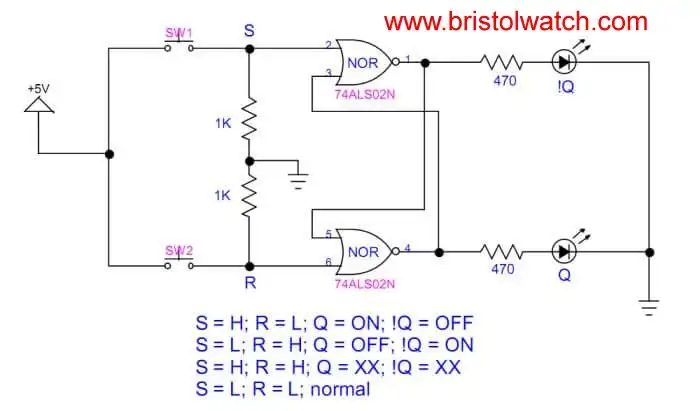
Fig. 1: Basic NOR gate SR latch circuit.
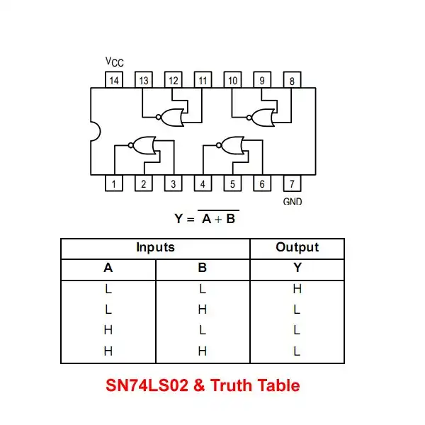
Fig. 2: 74LS02 pin connections and truth table.
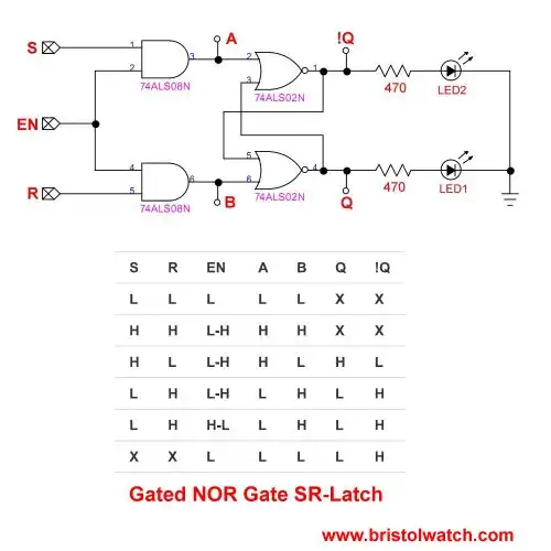
Fig. 3: Basic NOR gate gated SR latch truth table.
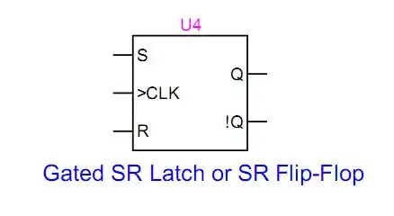
Fig. 4: Gated SR latch logic symbol.
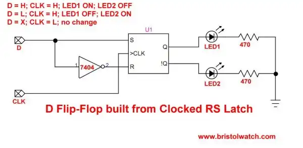
Fig. 5: SR latch and inverter form D flip-flop.
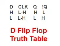
Fig. 6: D flip-flop truth table.
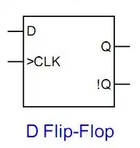
Fig. 7: D flip-flop symbol.
Digital Circuits & Logic Design Tutorials
Logic Gates, Latches & Flip-Flops
- Basic NAND Gate SR Latch Circuit
- Tutorial NOR Gate SR Latch Circuit
- SR Latch and Microcontroller I/O Pin Tutorial
- Tutorial OR-NOR Circuits Including Monostable Multivibrator
- Brief Tutorial of XOR and XNOR Logic Gates
- SN74HC14 Square Wave Generator uses SN7476 JK Flip-Flop
Timers, Oscillators & Pulse Generators
- Simple Schmitt Trigger SN74HC14 Square Wave Generator
- Three Output Pulse Generator Circuit for Digital Circuits
- Introduction to RC Differentiator Circuits and Uses
- LM555-NE555 One-Shot Multivibrator AC Power Control
- Astable CD4047 Geiger Counter Power Supply
- CD4047 Monostable Multivibrator Circuit
Power MOSFETs, Drivers & H-Bridge Motor Controls
- From Basic Digital Circuits to H-Bridge Motor Controls
- High-Current MOSFET Driver Circuits for Control Systems
- Non-Inverting Tri-State Buffer-Switch Demo Circuit
- Basic TTL Tri-State Buffer Circuit Examples
- Connecting Digital Logic to Power Transistors
- Optocouplers for TTL-CMOS Logic Level Shifting
- Driving Darlington Transistors with Optocouplers
- Tri-State H-Bridge Design Using Optocouplers
- H-Bridge Schematic with MOSFET Outputs
- H-Bridge Schematic with Darlington-MOSFET Transistor Outputs
- H-Bridge Schematic with Darlington-IGBT Transistor Outputs
- Test Power MOSFET Transistors, IGBTs Results, Observations
- Exploring Solid State Relays and Control Circuits
Video Resources
Search Electronics Projects
Other Circuits
- Hall Effect Magnetic Switches and Sensors
- Comparator Theory Circuits Tutorial
- ULN2003A Darlington Transistor Array with Circuit Examples
- Transistor-Zener Diode Regulator Circuits
- AC Power Supply Rectification
- Coils for Highly Selective Crystal Radio
- Neon (NE-2) Circuits You Can Build
- Photodiode Circuits Operation and Uses
- Photodiode Op-Amp Circuits Tutorial